Via structure having open stub and printed circuit board having the same

a technology of printed circuit board and open stub, which is applied in the formation of printed element electric connection, high frequency circuit adaptation, multiple-port network, etc., can solve the problems of deteriorating return loss characteristics and greater transmission loss value of signal transmission channels, so as to improve the transmission loss and return loss characteristics of signals

Active Publication Date: 2014-03-20
SAMSUNG ELECTRO MECHANICS CO LTD
View PDF4 Cites 17 Cited by
  • Summary
  • Abstract
  • Description
  • Claims
  • Application Information

AI Technical Summary

Benefits of technology

[0013]The present invention has been invented in order to overcome the above-described problems and it is, therefore, an object of the present invention ...

Problems solved by technology

The longer the line and the higher the frequency, the greater the transmission loss value of a signal transmission channel of the circuit board having t...

Method used


Image

  • Via structure having open stub and printed circuit board having the same
  • Via structure having open stub and printed circuit board having the same
  • Via structure having open stub and printed circuit board having the same

Examples


Embodiment Construction

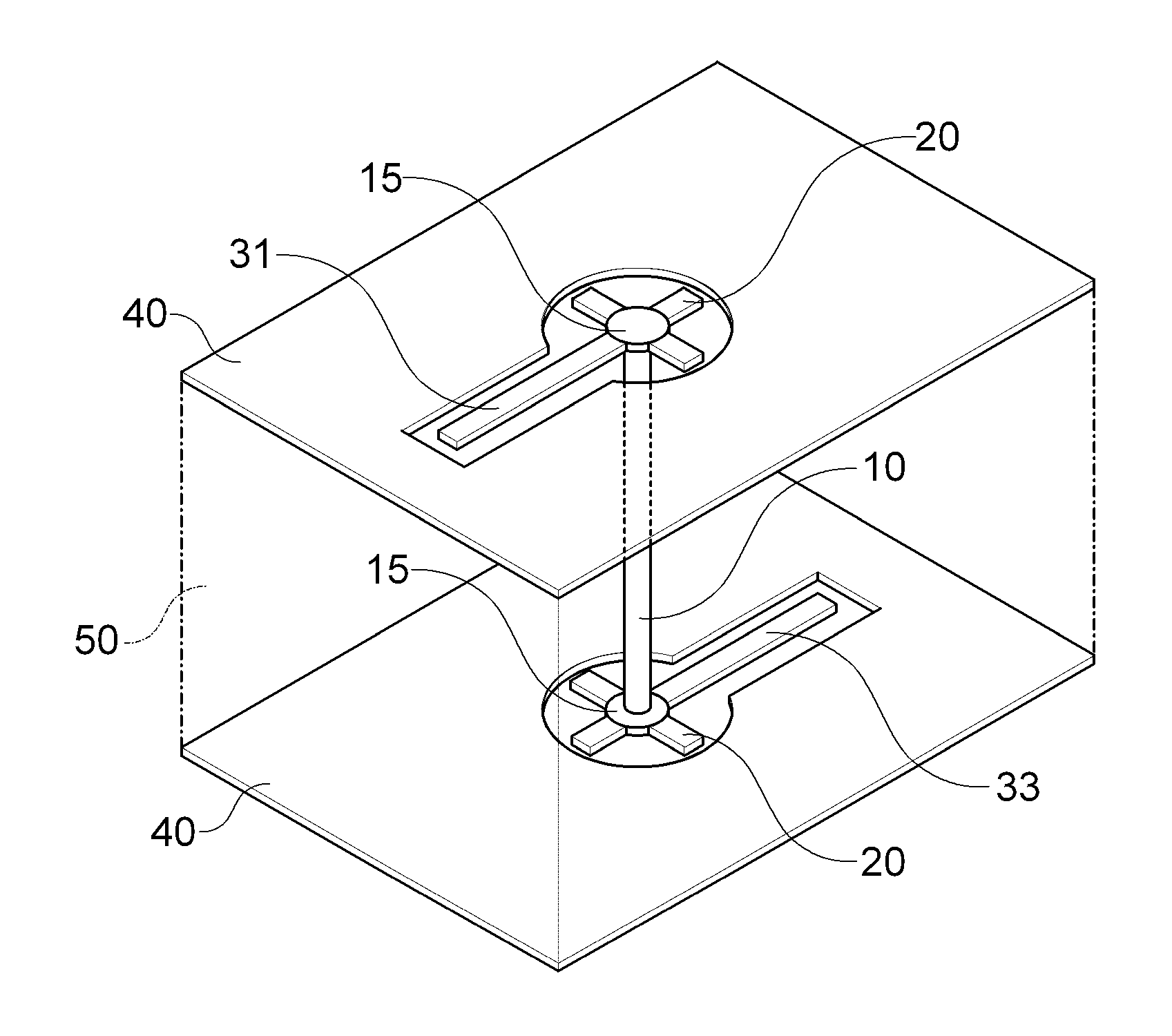
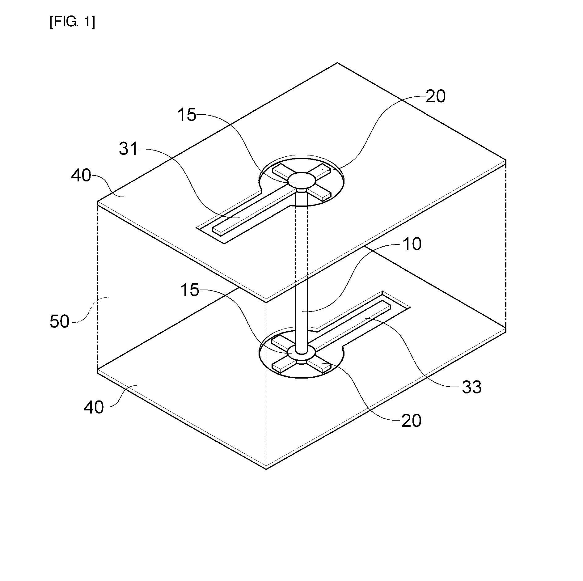
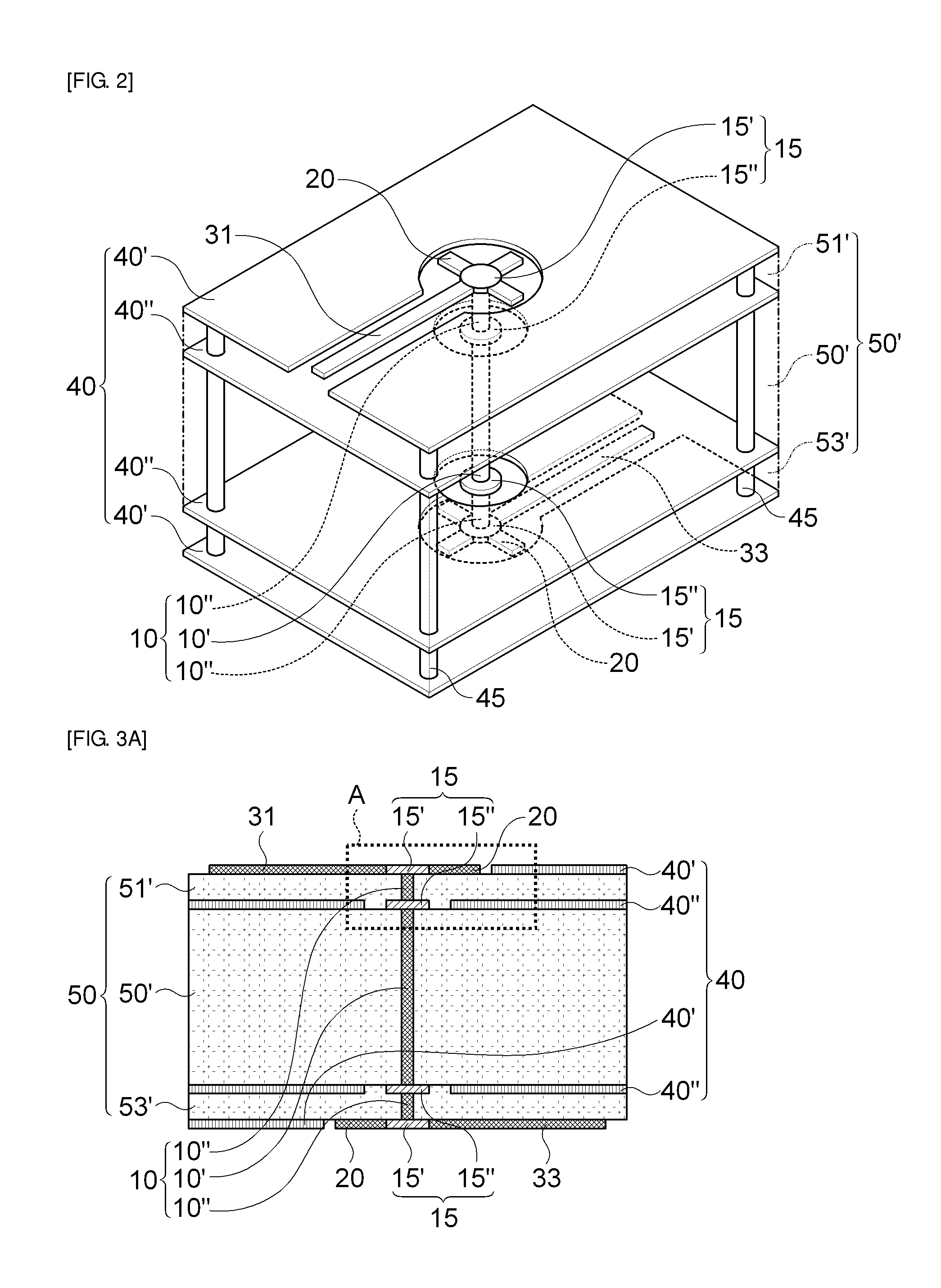
[0037]Embodiments of the present invention to achieve the above-described objects will be described with reference to the accompanying drawings. In this description, the same elements are represented by the same reference numerals, and additional description which is repeated or limits interpretation of the meaning of the invention may be omitted.

[0038]In this specification, when an element is referred to as being “connected or coupled to” or “disposed in” another element, it can be “directly” connected or coupled to or “directly” disposed in the other element or connected or coupled to or disposed in the other element with another element interposed therebetween, unless it is referred to as being “directly coupled or connected to” or “directly disposed in” the other element.

[0039]Although the singular form is used in this specification, it should be noted that the singular form can be used as the concept representing the plural form unless being contradictory to the concept of the ...


PUM


Abstract

The present invention relates to a via structure having an open stub and a printed circuit board having the same. In accordance with an embodiment of the present invention, a via structure having an open stub including: a signal transmission via passing through an insulating layer; upper and lower via pads for connecting first and second transmission lines, which are respectively formed on and under the insulating layer, and the signal transmission via; and at least one open stub connected to an outer periphery of each via pad to have a shunt capacitance with each ground pattern formed on and under the insulating layer is provided. Further, a printed circuit board with a via having an open stub is provided.

Description

CROSS-REFERENCE TO RELATED APPLICATIONS[0001]Claim and incorporate by reference domestic priority application and foreign priority application as follows:CROSS REFERENCE TO RELATED APPLICATION[0002]This application claims the benefit under 35 U.S.C. Section 119 of Korean Patent Application Serial No. 10-2012-0103421, entitled filed Sep. 18, 2012, which is hereby incorporated by reference in its entirety into this application.”BACKGROUND OF THE INVENTION[0003]1. Field of the Invention[0004]The present invention relates to a via structure having an open stub and a printed circuit board having the same, and more particularly, to a via structure having an open stub that has an open stub connected to a via pad, and a printed circuit board having the same.[0005]2. Description of the Related Art[0006]As the transmission rate of mobile devices such as PCs, mobile phones, and tablet PCs and the data rate increase, the amount of data transmitted through a circuit board and the usable frequenc...

Claims


Application Information

Patent Timeline
IPC IPC(8): H03H7/01
CPCH03H7/17H05K1/0251H05K1/116H05K2201/09381H05K3/40H05K3/46
Inventor LEE, DONG HWANPARK, SEUNG WOOKROMERO, CHRISTIANKWEON, YOUNG DOKIM, JIN GU
Owner SAMSUNG ELECTRO MECHANICS CO LTD
Why Eureka
Try Eureka