Liquid crystal display having multiple pixel regions for improved transmittance

a technology of liquid crystal display and transmittance, which is applied in non-linear optics, instruments, optics, etc., can solve the problems of difficult sidegray expression and deterioration of display quality, and achieve the effect of deterioration of transmittan

Active Publication Date: 2014-07-31
SAMSUNG DISPLAY CO LTD
View PDF3 Cites 25 Cited by
  • Summary
  • Abstract
  • Description
  • Claims
  • Application Information

AI Technical Summary

Benefits of technology

[0013]The present invention provides a liquid crystal display having advantages of expressing more accurate gray in a low gray region and preventing transmittance deterioration while side visibility is close to front visibility.
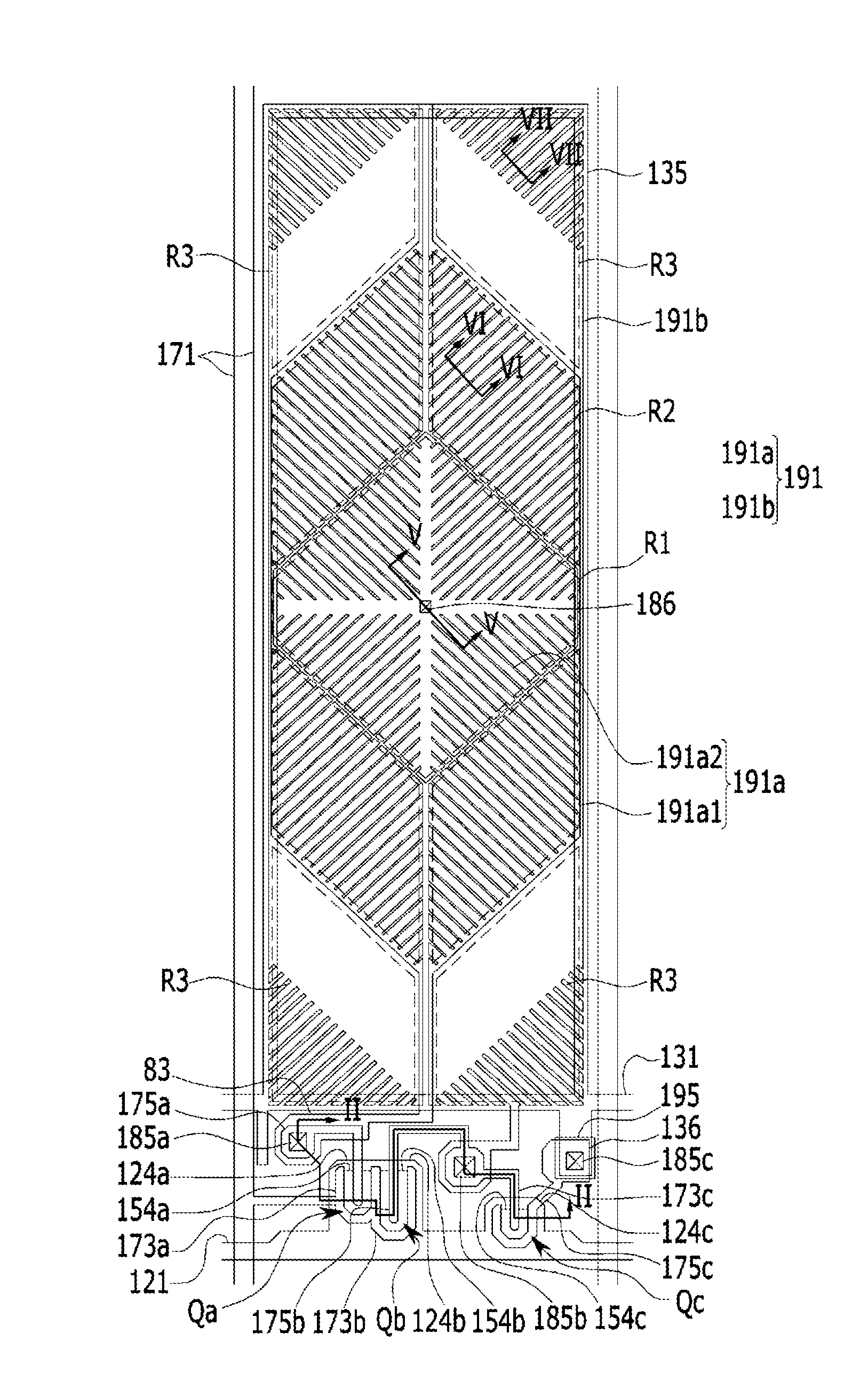
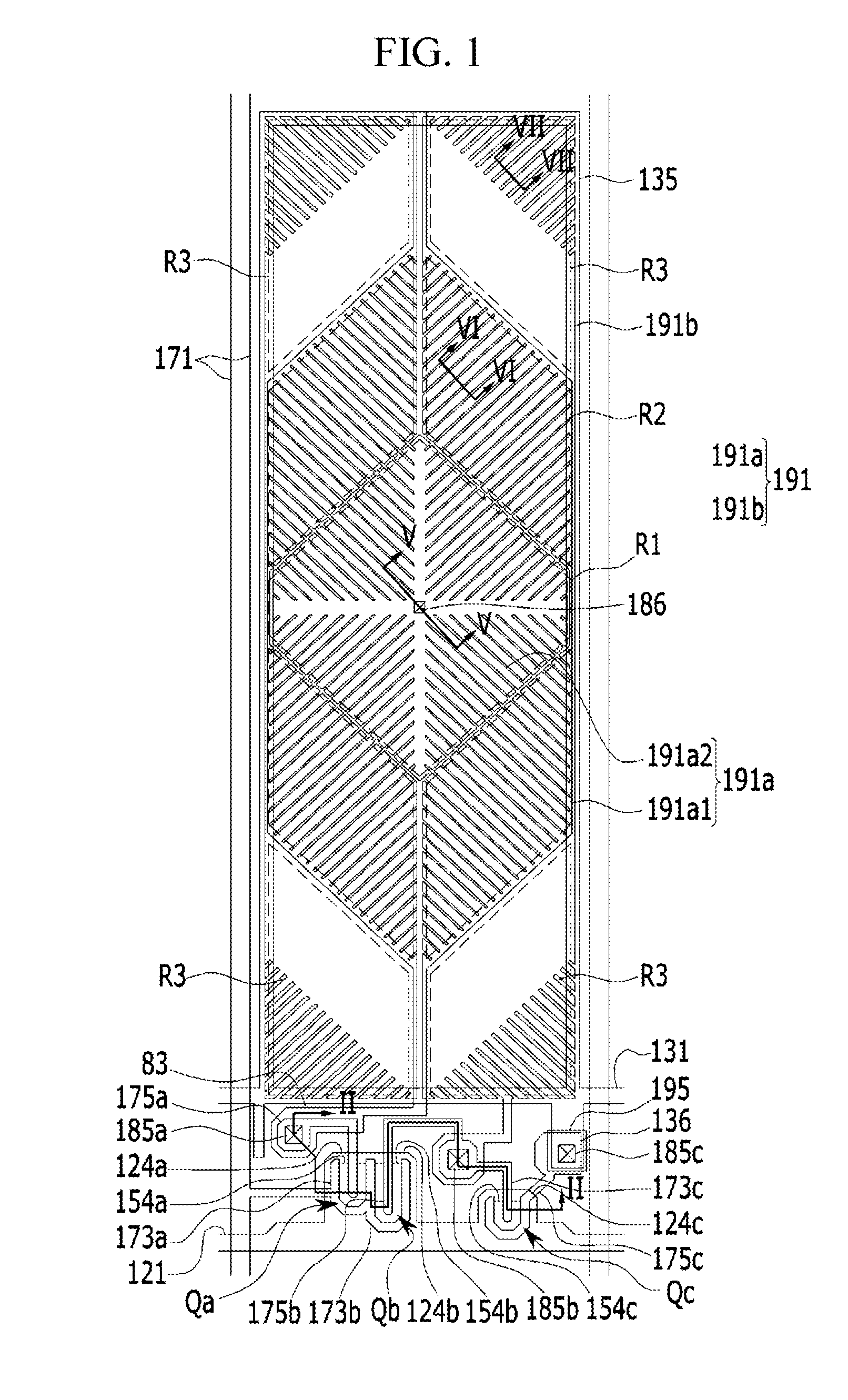
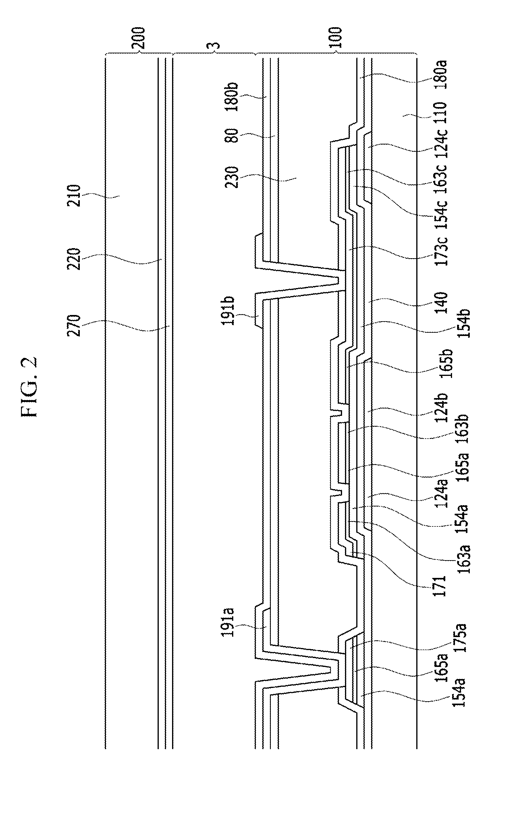
[0027]In the liquid crystal display according to an exemplary embodiment of the present invention, a first subpixel electrode and a second subpixel electrode are formed, and a portion of the first subpixel electrode and a portion of the second subpixel electrode overlap each other to divide one pixel area into a first region containing the first subpixel electrode (but not the second subpixel electrode), a second region containing an area of overlap between the first subpixel electrode and the second subpixel electrode, and a third region containing the second subpixel electrode (but not the first subpixel electrode). Accordingly, an accurate gray in a low gray region may be realized along with side visibility that is close to front visibility, and transmittance deterioration that may be generated in the region between the first subpixel electrode and the second subpixel electrode may be reduced or prevented.

Problems solved by technology

However, when approximating the side visibility to the front visibility by dividing one pixel into two subpixels and forming different transmittances, the luminance is increased at a low gray or high gray such that gray expression is difficult at the sides, thereby deteriorating display quality.

Method used


Image

  • Liquid crystal display having multiple pixel regions for improved transmittance
  • Liquid crystal display having multiple pixel regions for improved transmittance
  • Liquid crystal display having multiple pixel regions for improved transmittance

Examples


Embodiment Construction

[0052]Exemplary embodiments of the present invention will be described in detail with reference to the attached drawings. The present invention may be modified in many different forms, and should not be construed as being limited to the exemplary embodiments set forth herein. Rather, the exemplary embodiments of the present invention are provided so that this disclosure will be thorough and complete, and will fully convey the concept of the present invention to those skilled in the art.

[0053]In the drawings, the thickness of layers and regions may be exaggerated for clarity. In addition, when a layer is described to be formed on another layer or on a substrate, this means that the layer may be formed on the other layer or on the substrate, or a third layer may be interposed between the layer and the other layer or the substrate. Like numbers refer to like elements throughout the specification. The drawings are not necessarily to scale. Any combination and / or permutation of any of th...


PUM

PropertyMeasurementUnit
angleaaaaaaaaaa
voltageaaaaaaaaaa
areaaaaaaaaaaa

Abstract

A liquid crystal display according to an exemplary embodiment of the present invention includes: a first substrate; a first subpixel electrode positioned on the first substrate and configured to receive a first voltage; a second subpixel electrode positioned on the first substrate and configured to receive a second voltage; an insulating layer positioned between the first subpixel electrode and the second subpixel electrode; a second substrate facing the first substrate; and a common electrode positioned on the second substrate. A portion of the first subpixel electrode and a portion of the second subpixel electrode overlap each other with the insulating layer interposed therebetween, and a difference between the first voltage and a common voltage is larger than a difference between the second voltage and the common voltage.

Description

CROSS-REFERENCE TO RELATED APPLICATION[0001]This application claims priority to, and the benefit of, Korean Patent Application No. 10-2013-0010639 filed in the Korean Intellectual Property Office on Jan. 30, 2013, the entire contents of which are incorporated herein by reference.BACKGROUND OF THE INVENTION[0002](a) Technical Field[0003]Embodiments of the present invention relate generally to flat panel displays. More specifically, embodiments of the present invention relate to liquid crystal displays having multiple pixel regions for improved transmittance.[0004](b) Description of the Related Art[0005]A liquid crystal display, which is one of the most common types of flat panel displays currently in use, includes two panels with field generating electrodes such as a pixel electrode, a common electrode, and the like, with a liquid crystal layer interposed therebetween.[0006]The liquid crystal display generates an electric field in the liquid crystal layer by applying a voltage to the...

Claims


Application Information

Patent Timeline
Patent Type & Authority Applications(United States)
IPC IPC(8): G02F1/1343
CPCG02F1/134336G02F1/133707G02F1/134309G02F1/13624G02F2203/30G02F2203/64G02F1/133742G02F1/134345G02F1/13712G02F1/1343
Inventor KIM, HOONKIM, SU JEONGSHIN, KI CHULYANG, DAN BIJUNG, JAE-HOONHAN, MIN JUHONG, JI PHYO
Owner SAMSUNG DISPLAY CO LTD
Why Eureka
Try Eureka