Input function display device

a display device and function technology, applied in the field of input function display devices, can solve the problems of increasing the thickness of the device, narrowing the display area, and deteriorating the display contrast by about 10%, so as to reduce the display quality and narrow the display area

Active Publication Date: 2015-10-27
E INK CORPORATION
View PDF19 Cites 3 Cited by
  • Summary
  • Abstract
  • Description
  • Claims
  • Application Information

AI Technical Summary

Benefits of technology

[0011]An advantage of some aspects of the invention is to provide an input function display device in which a decrease of display quality and narrowing of a display area are suppressed and to cause the device to be thin.
[0013]With such a configuration, while moving the position information reading unit in a display area (input face) where a coordinate system is defined, the display is performed at a part designating the position, and thus it is possible to perform handwriting input to the display portion (display area) of the display unit. In the invention, the conductive pattern to which the position information pattern is applied serves (also) as the common electrode of the display portion, it is not necessary to provide the conductive pattern separately from the common electrode, and thus it is possible to reduce the thickness of the device. Because the common electrode also serves as the conductive pattern, it is possible to prevent transmittance from decreasing. In the invention, by using the method of optically reading the position information pattern while capturing an image of the position information pattern using the position information reading unit, there is no worry that electrical noise occurs, and it is not necessary to mount the LED and the photo sensor in the peripheral portion of the display area as described in the related art. Accordingly, it is possible to prevent the display area from being narrow, and to reduce the thickness of the device without decreasing the display quality.
[0015]With such a configuration, it is possible to accurately understand the position of the display area using characteristics (unique value) of the M plane.
[0019]With such a configuration, it is possible to detect only the position information pattern except for the background light of the display portion, and thus it is possible to obtain accurate position information. An S / N ratio caused by periphery environment light (visible light or the like) is prevented from being decreased, and thus it is possible to read the position information pattern.
[0023]With such a configuration, it is possible to keep the display contents even when the power supply from the outside is stopped, and thus it is possible to obtain the input function display device capable of achieving low power consumption.
[0025]With such a configuration, it is possible to keep the display contents even when the power supply from the outside is stopped, and thus it is possible to obtain the input function display device capable of achieving low power consumption.

Problems solved by technology

However, a display contrast deteriorates by about 10% due to transmittance or reflectance of the transparent electrodes.
However, in the optical type, since the LED or photo sensor is mounted on a peripheral portion of the display body and it is necessary to secure a light path, the display area becomes narrow and the thickness of the device is increased.
In addition, there is a supersonic wave type which measures a retuning time of a supersonic wave to detect a position, but, as with the optical type, there is a problem in that the display area becomes narrow and the thickness of the device is increased.
The technique disclosed in JP-A-2005-302508 is proposed as the transparent conductive sheet for the resistive film touch panel, at least two opposed sheets are necessary, and there is a drawback that it may not be also used in a common electrode of a display body from the influence of noise.
The technique disclosed in JP-A-2006-330649 is limited to a specific display body or driving circuit, a lot of emission lightings are necessary in a periphery of a display body, and thus there are concerns about the narrowing of the display area and an increase of the thickness of the device.
The technique disclosed in JP-A-2002-196875 does not achieve sharing of an electrode layer with a coordinate plate and a display body similarly to the touch panel of the related art, and there are concerns of a decrease in transmittance.
Even in JP-A-63-70326, it is difficult to reduce a size of a device, due to having a configuration in which an antenna substrate is provided under display body.

Method used


Image

  • Input function display device
  • Input function display device
  • Input function display device

Examples


first embodiment

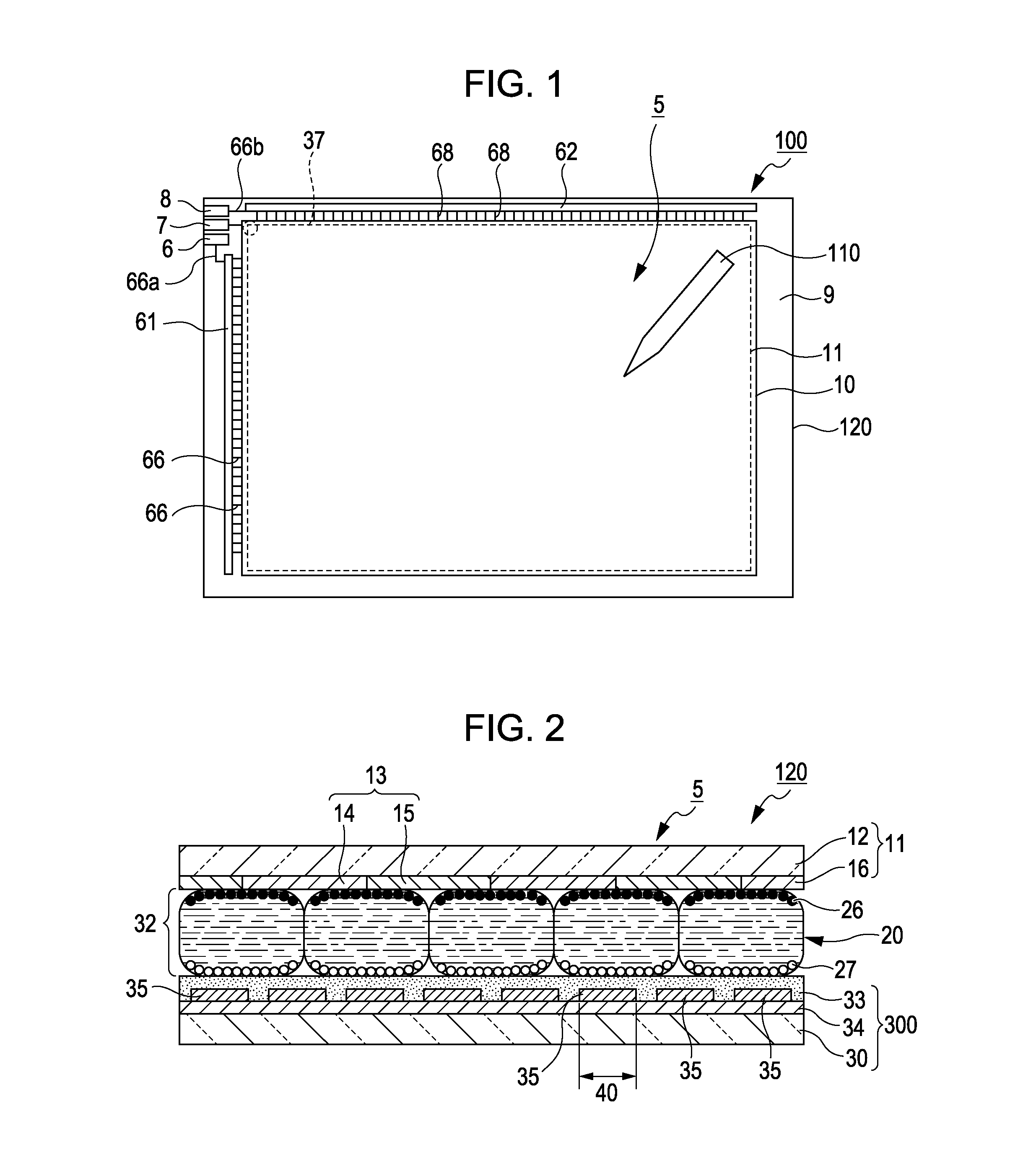
[0036]FIG. 1 is a plan view illustrating an overall configuration of an input function display device of the invention. FIG. 2 is a cross-sectional view illustrating a schematic configuration of a display body in the input function display device.

[0037]As shown in FIG. 1 and FIG. 2, the input function display device 100 includes an electronic pen (position information reading unit) 110, and a display body (display unit) 120, and is a display device which can perform handwriting input to a display face of the display body 120 using the electronic pen 110. Herein, handwriting information is displayed by acquiring time series data of a contact point of the electronic pen 110 to the display face of the display body 120 using the position information pattern 16 as a unit that detects position information (coordinate value in change of time) of the electronic pen 110 of the display body 120.

[0038]The display body 120 is formed of a display body (display portion) 10 having a coordinate bod...

example 1

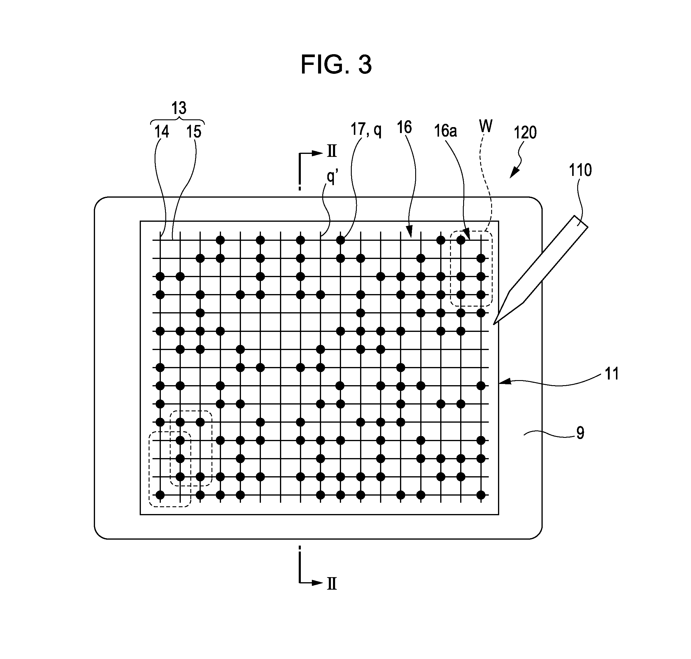
[0074]FIG. 5A is diagram illustrating a position information pattern in Example 1, and FIG. 5B and FIG. 5C are diagrams illustrating a relationship between quadrants and marks at the reference position.

[0075]As shown in FIG. 5A, the position information pattern 19 is configured by the dots 18 assigned to the plurality of intersection points of the thin line patterns 14 and 15, represents a numerical value [0] at the intersection point where no dot 18 is provided, and represents numerical values [0] to [3] according to the number and the disposition of dots 18 at the intersection point areas, at the intersection points where the dots 18 are provided.

[0076]The position information pattern 19 has a reference position corresponding to the intersection point of the conductive pattern 13, and an arbitrary numerical value (coordinate value) is determined by the existence and nonexistence of the dots 18 or the disposition of the dot 18 with respect to the reference position. The shape of a ...

example 2

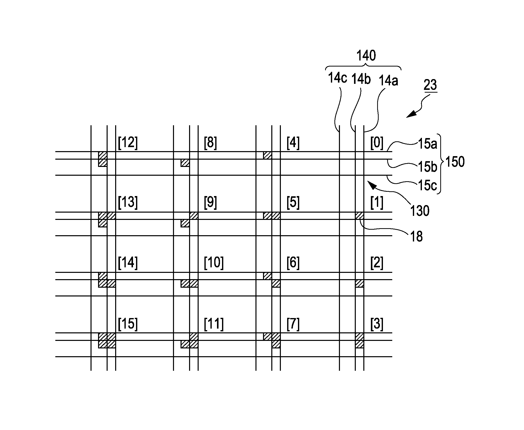
[0080]FIG. 6 is a diagram illustrating a position information pattern in Example 2.

[0081]As shown in FIG. 6, the position information pattern 23 in the example has a conductive pattern 130 in which a thin line pattern (first thin line pattern) 140 with one set of three thin lines 14a, 14b, and 14c and a thin line pattern 150 with one set of three thin lines 15a, 15b, and 15c (second thin line pattern) are arranged in a lattice shape, and it is possible to identify a rotation state of the conductive pattern 130 by asymmetry between pitch widths of the thin lines 14a, 14b, and 14c and pitch widths of the thin lines 15a, 15b, and 15c.

[0082]The reference position of the position information pattern 23 is regulated by the intersection point of the thin lines 14b and 15b of the thin line patterns 140 and 150 intersecting with each other, and the coordinate value is represented by the disposition of the dots 18 with respect to the reference position.

[0083]The coordinate value is encoded b...


PUM


Abstract

An input function display device includes: a position information reading unit that is provided with an imaging element optically reading a position information pattern representing a coordinate position on a plane; and a display unit that performs display on the basis of marks read from the position information pattern recorded in a display area, wherein the display unit includes a transparent conductive film having a conductive pattern in which the position information pattern is applied onto the transparent substrate, and a display portion that performs display using the conductive pattern as a common electrode.

Description

BACKGROUND[0001]1. Technical Field[0002]The present invention relates to an input function display device.[0003]2. Related Art[0004]Recently, a transparent conductive film has been developed in which a thin line pattern (conductive pattern) of metal or a conductive material is printed on a resin film, as a magnetic shield of a display or a transparent electrode for a resistive film touch panel. There are expectations for this as new technology to replace an ITO conductive film, for which there are concerns of depletion of earth's resources.[0005]As a general related art of the touch panel and pen input, there is a resistive film type and a capacitive detection type using transparent electrodes. However, a display contrast deteriorates by about 10% due to transmittance or reflectance of the transparent electrodes. Particularly, in a mobile apparatus, there are many cases where a reflectance display body with low power consumption is used to extend a battery life, and display quality ...

Claims


Application Information

Patent Timeline
Patent Type & Authority Patents(United States)
IPC IPC(8): G06F3/042G06F3/0354G06F3/03G06K9/22G09G3/34
CPCG06F3/03542G06F3/0317G06K9/222G06K2009/226G09G3/344G09G2300/0426G06F3/0321G06V30/1423G06V10/19
Inventor TAKEDA, KEIGO
Owner E INK CORPORATION
Why Eureka
Try Eureka