Method and system for three-dimensional (3D) structure fill

a technology of structure filling and three-dimensional filling, applied in the field of three-dimensional (3d) structure filling, can solve the problems of reducing the performance and yield of the device formed, the process of filling trenches becomes more difficult, and the device performance is poor

Active Publication Date: 2015-04-02
APPLIED MATERIALS INC
View PDF2 Cites 26 Cited by
  • Summary
  • Abstract
  • Description
  • Claims
  • Application Information

AI Technical Summary

Benefits of technology

[0008]One or more embodiments of the invention are direc

Problems solved by technology

As trench widths become narrower and trench aspect ratios increase, the process of filling trenches becomes more challenging.
Impurities in the filled trenches can reduce performance and yield of devices formed with the filled trenches.
The uneven deposition forms

Method used


Image

  • Method and system for three-dimensional (3D) structure fill
  • Method and system for three-dimensional (3D) structure fill
  • Method and system for three-dimensional (3D) structure fill

Examples


Embodiment Construction

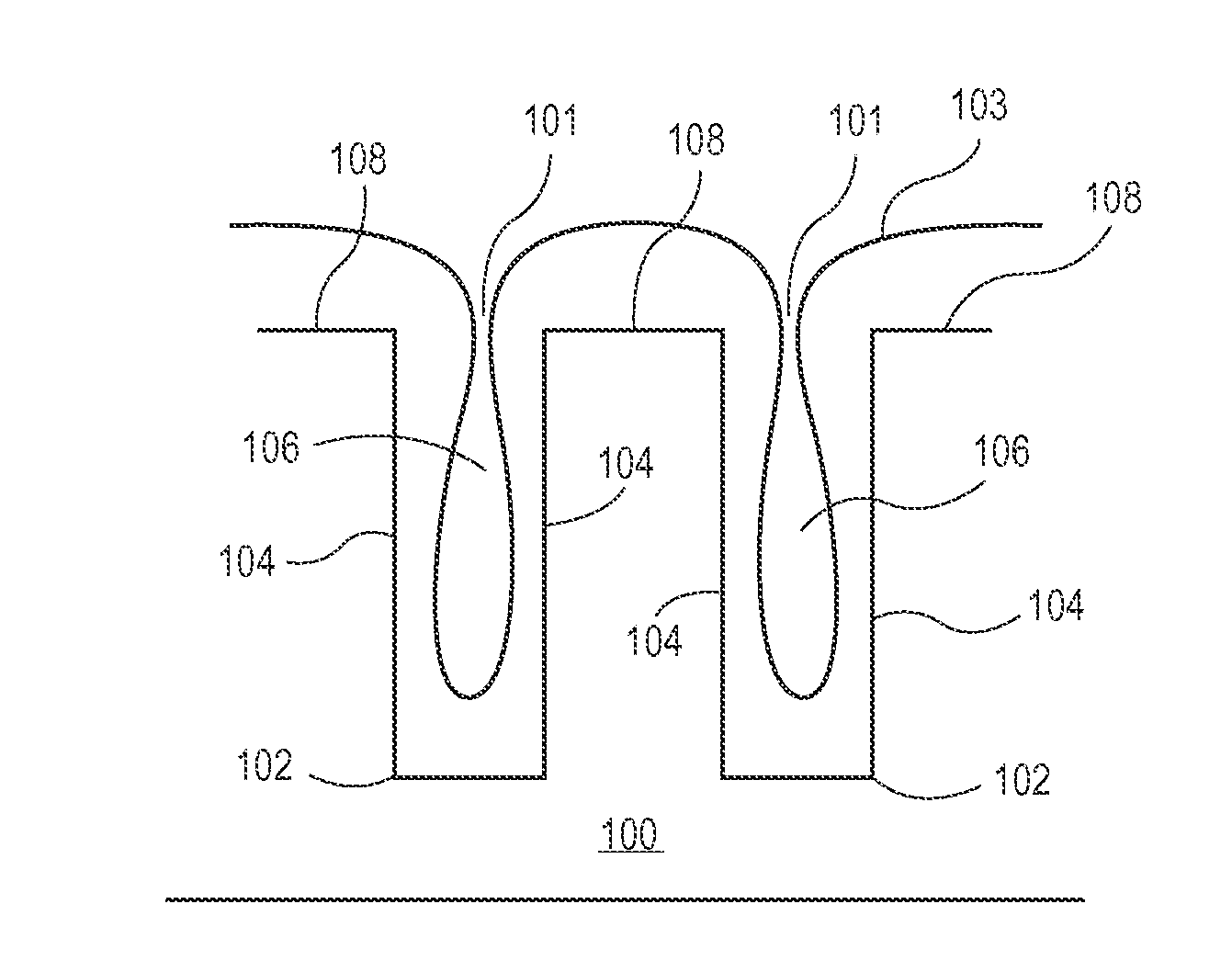
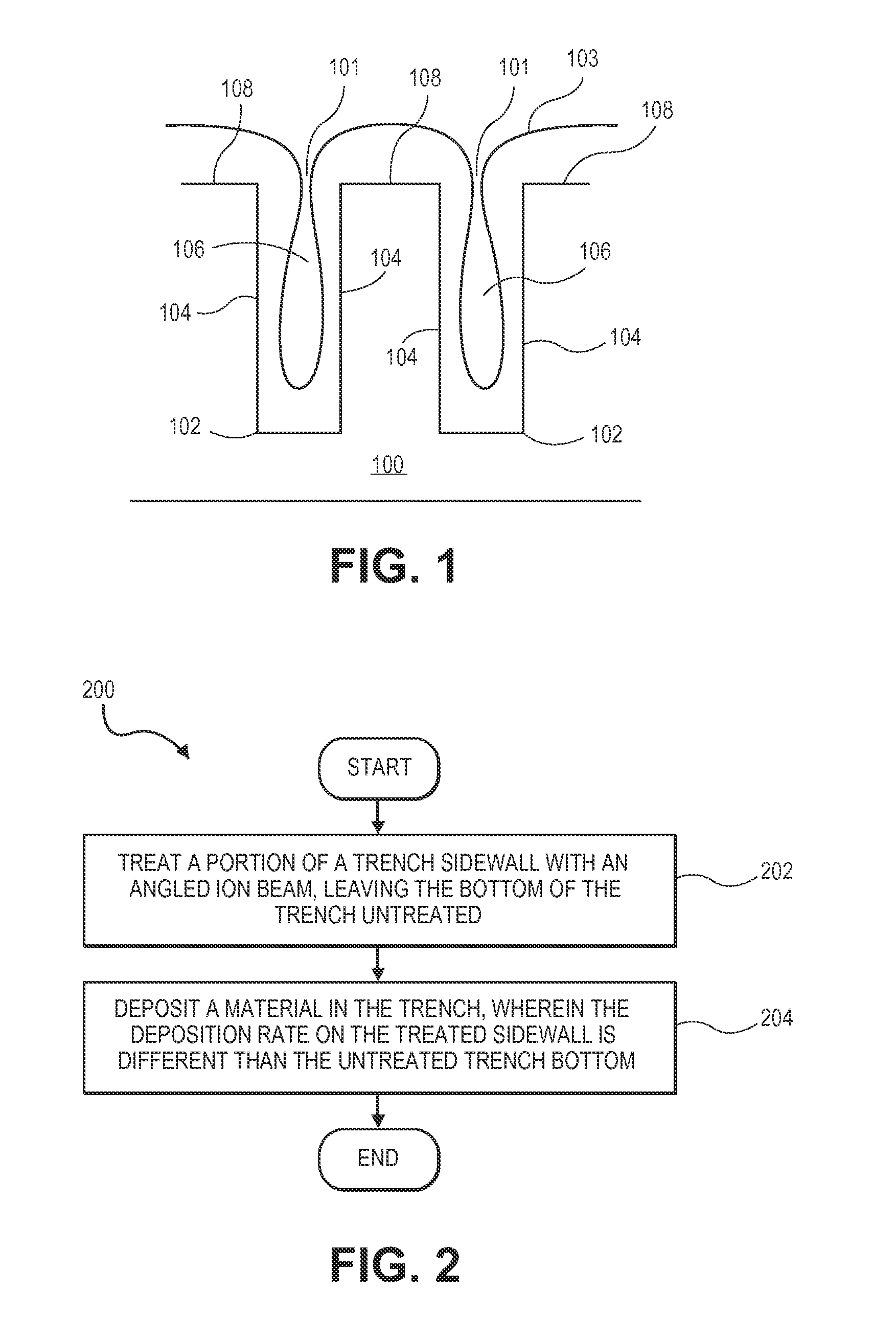
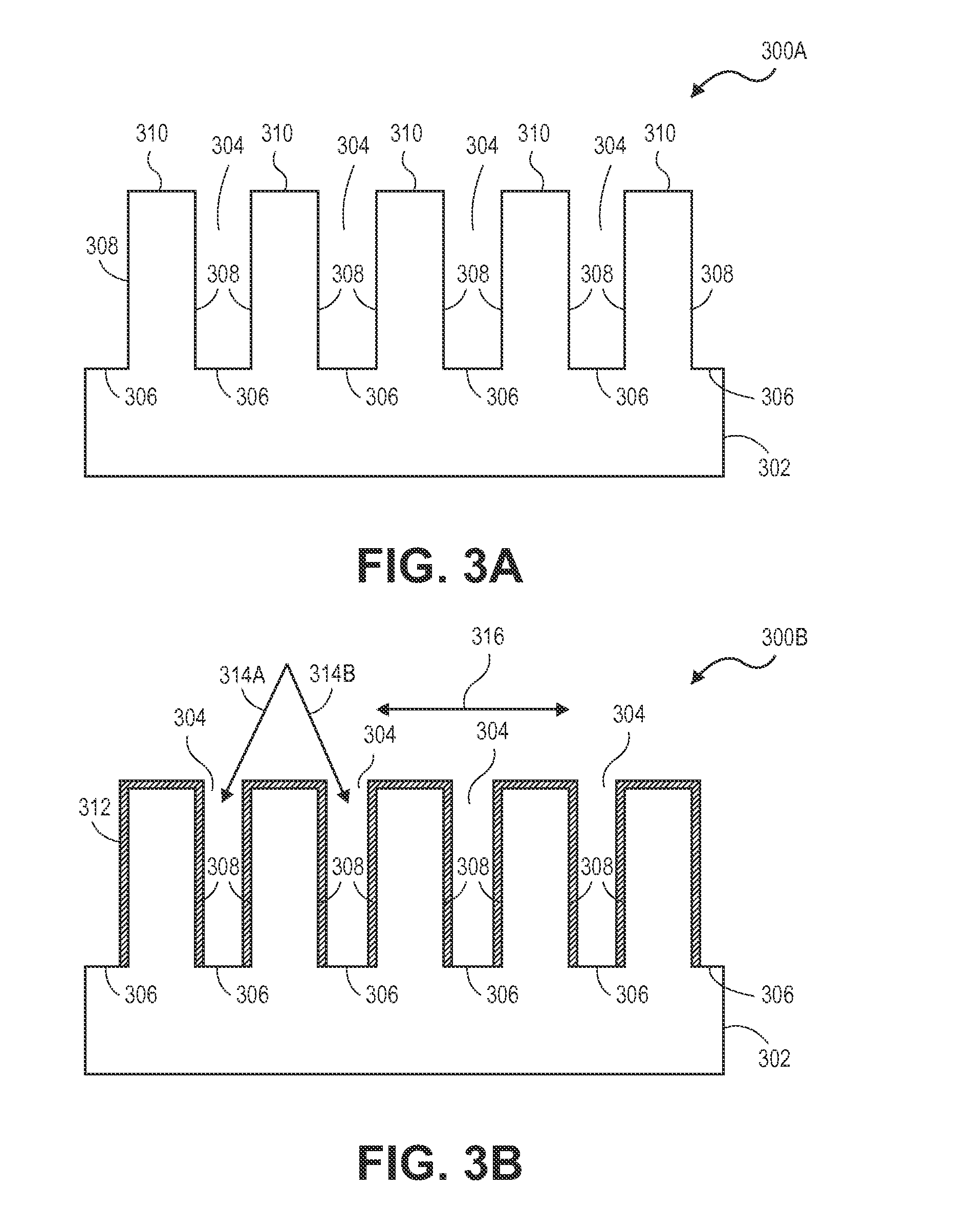
[0024]Apparatuses, systems, and methods of three-dimensional structure fill are described. Three-dimensional structure fill can include filling trenches in a semiconductor wafer or substrate with a material, also known as gap fill. The term “trench” is used in the following description to refer to any hole or other three-dimensional structure capable of being filled in a semiconductor wafer or substrate.

[0025]Embodiments of the invention involve the use of one or more angled ion beams to treat portions of trench sidewalls to change the deposition rate of fill materials on the treated portions. A treated “portion” of a sidewall may include the entire sidewall, or less than the entire sidewall. The angled ion beams can treat part or all of the trench sidewalls without treating the trench bottom. The deposition rate of fill materials on the treated portions can be lower than the untreated bottoms, resulting in bottom-up fill without the formation of overhangs at the trench opening, or ...


PUM

PropertyMeasurementUnit
Fractionaaaaaaaaaa
Fractionaaaaaaaaaa
Angleaaaaaaaaaa

Abstract

Embodiments include methods and systems of 3D structure fill. In one embodiment, a method of filling a trench in a wafer includes performing directional plasma treatment with an ion beam at an angle with respect to a sidewall of the trench to form a treated portion of the sidewall and an untreated bottom of the trench. A material is deposited in the trench. The deposition rate of the material on the treated portion of the sidewall is different than a second deposition rate on the untreated bottom of the trench. In one embodiment, a method includes depositing a material on the wafer, filling a bottom of the trench and forming a layer on a sidewall of the trench and a top surface adjacent to the trench. The method includes etching the layer with an ion beam at an angle with respect to the sidewall.

Description

BACKGROUND[0001]1) Field[0002]Embodiments of the present invention pertain to the field of semiconductor processing and, in particular, to methods of three-dimensional (3D) structure fill.[0003]2) Description of Related Art[0004]Semiconductor wafer processing may involve forming and filling trenches in semiconductor wafers or substrates. Filling trenches in a semiconductor wafer or substrate with a material may be referred to as “gap fill.” Gap fill is used in a variety of applications, such as in the formation of through-silicon vias (TSVs). As trench widths become narrower and trench aspect ratios increase, the process of filling trenches becomes more challenging.[0005]One existing gap fill method is spin-coating. Spin-coating typically involves coating a wafer or substrate with a liquid material with a spin-coating machine. Spin-coating machines may include a spin track that holds and rotates the wafer or substrate, and a nozzle at the center of the spin track that dispenses the ...

Claims


Application Information

Patent Timeline
IPC IPC(8): H01L21/02H01L21/67
CPCH01L21/67017H01L21/02104C23C14/021C23C14/046C23C16/0227C23C16/045H01J37/32009H01L21/02271H01L21/02315H01L21/67213H01L21/76224C23C16/45544C23C16/50H01J2237/334H01L21/02266H01L21/02274H01L21/0228H01L21/2855H01L21/28556H01L21/31116H01L21/32136
Inventor YIEH, ELLIEGODET, LUDOVICNEMANI, SRINIVASPING, ER-XUANDICKERSON, GARY
Owner APPLIED MATERIALS INC
Why Eureka
Try Eureka