
Ferroelectric semiconductor device and method of manufacturing the same

a technology of ferroelectric semiconductors and semiconductors, applied in the direction of semiconductor devices, basic electric elements, electrical equipment, etc., can solve the problem that ferroelectric materials can exhibit polarization hysteresis behavior

Active Publication Date: 2019-11-14
SK HYNIX INC
View PDF6 Cites 8 Cited by
  • Summary
  • Abstract
  • Description
  • Claims
  • Application Information

AI Technical Summary

Benefits of technology

This patent describes a new type of semiconductor device that uses a special material called ferroelectric to create a layer of memory. The device includes a channel structure with a trench pattern and a bottom surface and sidewall surface. A layer of insulating material is placed on top of the trench pattern, and a layer of ferroelectric material is placed on top of the insulating material. The ferroelectric material is then crystallized to form a patterned layer of memory, while the insulating material is left unchanged. This new device can allow for more efficient and reliable memory storage. The manufacturing process involves a series of steps to create the completed device.

Problems solved by technology

In addition, the ferroelectric material can exhibit a polarization hysteresis behavior when an external electric field is applied.

Method used


Image

  • Ferroelectric semiconductor device and method of manufacturing the same
  • Ferroelectric semiconductor device and method of manufacturing the same
  • Ferroelectric semiconductor device and method of manufacturing the same

Examples


Embodiment Construction

[0017]Various embodiments will now be described hereinafter with reference to the accompanying drawings. In the drawings, the dimensions of layers and regions may be exaggerated for clarity of illustration. The drawings are described with respect to an observer's viewpoint. If an element is referred to be located on another element, it may be understood that the element is directly located on the other element, or an additional element may be interposed between the element and the other element. The same reference numerals refer to the same elements throughout the specification.

[0018]In addition, expression of a singular form of a word should be understood to include the plural forms of the word unless clearly used otherwise in the context. It will be understood that the terms “comprise”, “include” or “have” are intended to specify the presence of a feature, a number, a step, an operation, an element, a part, or combinations thereof, but not used to preclude the presence or possibil...


PUM


Abstract

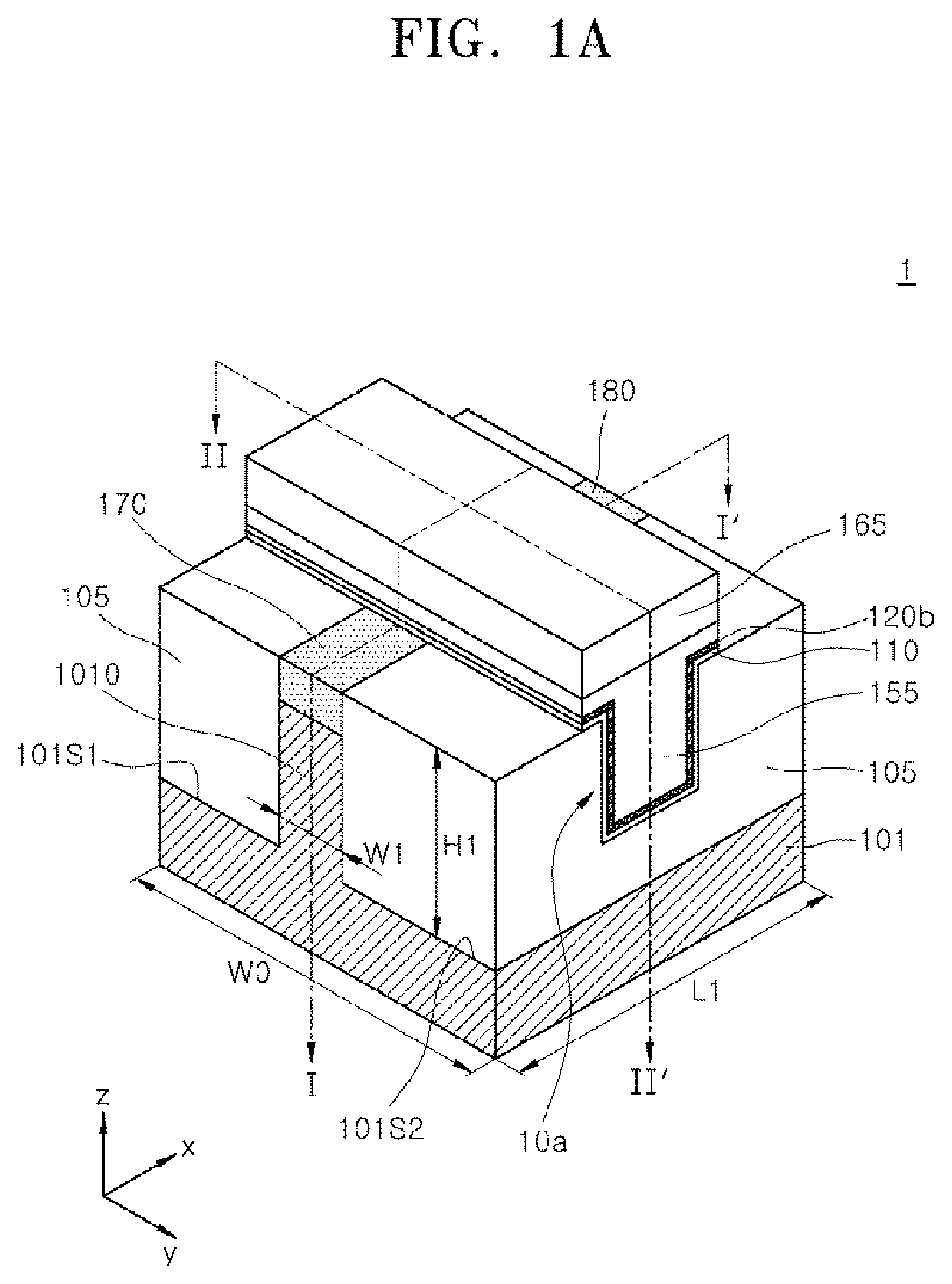
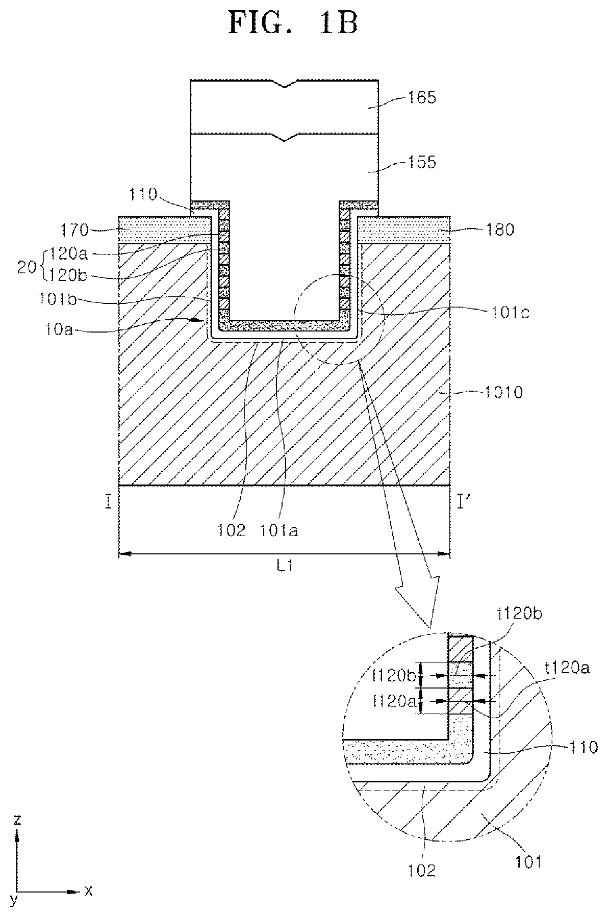
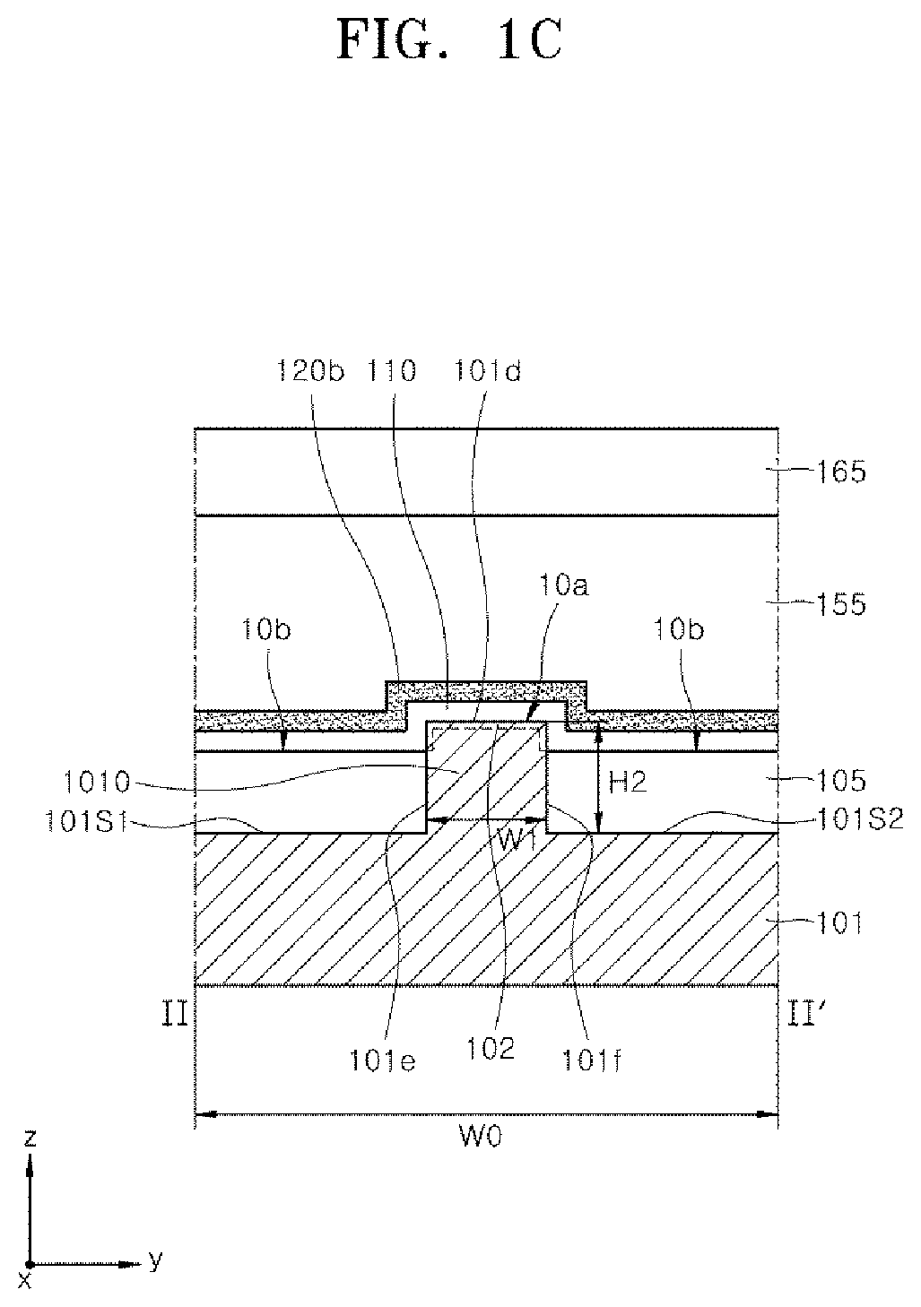
A ferroelectric semiconductor device of the present disclosure includes a substrate having a channel structure, a trench pattern having a bottom surface and a sidewall surface in the channel structure, a dielectric layer disposed on the bottom surface and the sidewall surface of the trench pattern, and a gate electrode layer disposed on the dielectric layer. The dielectric layer includes a ferroelectric layer pattern and a non-ferroelectric layer pattern that are disposed along the sidewall surface of the trench pattern.

Description

CROSS-REFERENCE TO RELATED APPLICATION[0001]The present application claims priority under 35 U.S.C. 119(a) to Korean Patent Application No. 10-2018-0053957, filed on May 10, 2018, which is herein incorporated by reference in its entirety.BACKGROUND1. Technical Field[0002]Various embodiments of the present disclosure generally relate to a semiconductor device, and more particularly, relate to a ferroelectric semiconductor device and a method of manufacturing the same.2. Related Art[0003]Generally, a ferroelectric material refers to a material having spontaneous electrical polarization in a state in which no external electric field is applied. In addition, the ferroelectric material can exhibit a polarization hysteresis behavior when an external electric field is applied. At this time, the applied electric field can be controlled so that the ferroelectric material has any one of two stable remanent polarization states on the polarization hysteresis curve. Such characteristic can be ut...

Claims


Application Information

Patent Timeline
Patent Type & Authority Applications(United States)
IPC IPC(8): H01L29/78H01L29/51H01L29/08H01L29/66H10B51/00
CPCH01L29/516H01L29/78391H01L27/11585H01L29/6684H01L29/0847H01L29/512H01L29/785H01L29/66795H01L29/40111H01L29/4236H01L21/0242H01L21/02181H01L21/02189H01L21/3213H10B51/00
Inventor YOO, HYANGKEUN
Owner SK HYNIX INC
Learn More