Semiconductor package structure and manufacturing method thereof

Inactive Publication Date: 2021-02-18
POWERTECH TECHNOLOGY
View PDF1 Cites 1 Cited by
  • Summary
  • Abstract
  • Description
  • Claims
  • Application Information

AI Technical Summary

Benefits of technology

[0004]The present invention provides a semiconductor package structure and a manufacturing method thereof for enhancing the electr

Problems solved by technology

In terms of a multi-function semiconductor package, how to enhance the electrical capability and/or performance of the semicondu

Method used


Image

  • Semiconductor package structure and manufacturing method thereof
  • Semiconductor package structure and manufacturing method thereof
  • Semiconductor package structure and manufacturing method thereof

Examples


Example

[0015]The directional terms used herein (for example, up, down, right, left, front, back, top, and bottom) are only for referencing to the drawings and are not intended to imply absolute directions.

[0016]Unless otherwise specifically stated, the steps of any method described herein are not intended to be construed as requiring execution in a particular order.

[0017]The present invention will be more comprehensively expounded with reference to the drawings of the embodiments. However, the present invention may also be embodied in a variety of different forms and should not be limited to the embodiments described herein. The thickness, dimensions, or size of layers or regions in the drawings are enlarged for clarity. The same or similar reference numerals denote the same or similar elements, which will not be reiterated one by one in the following paragraphs.

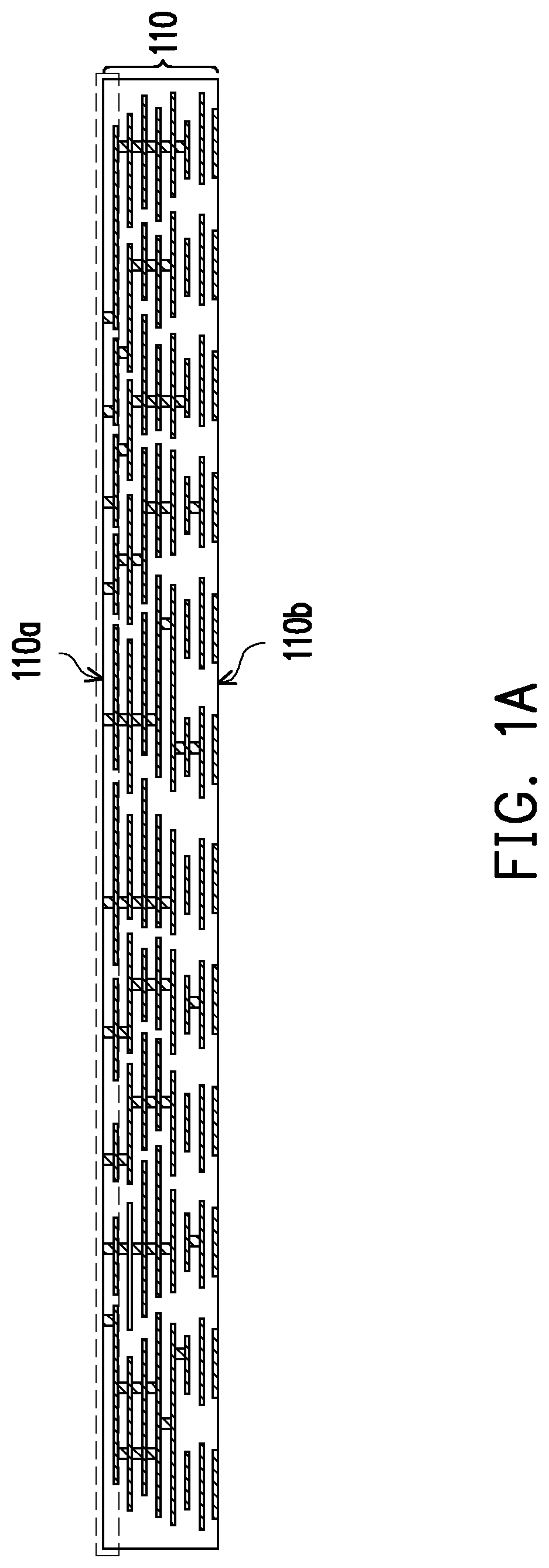
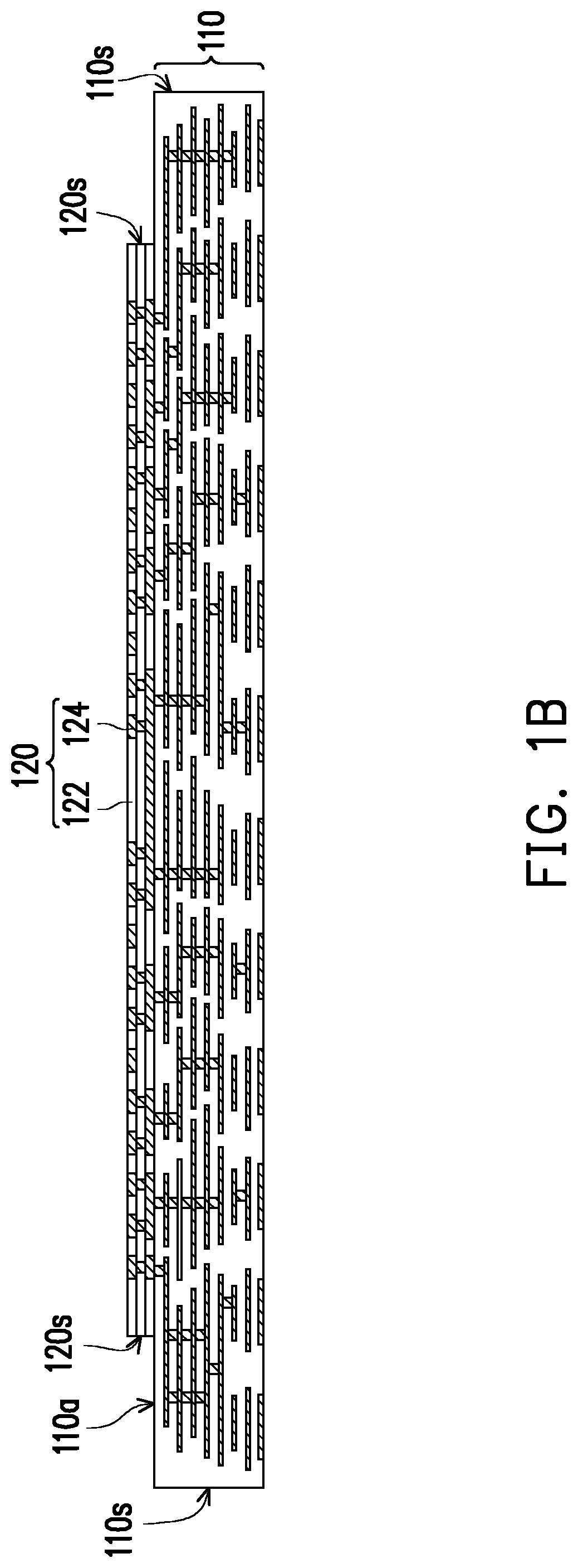
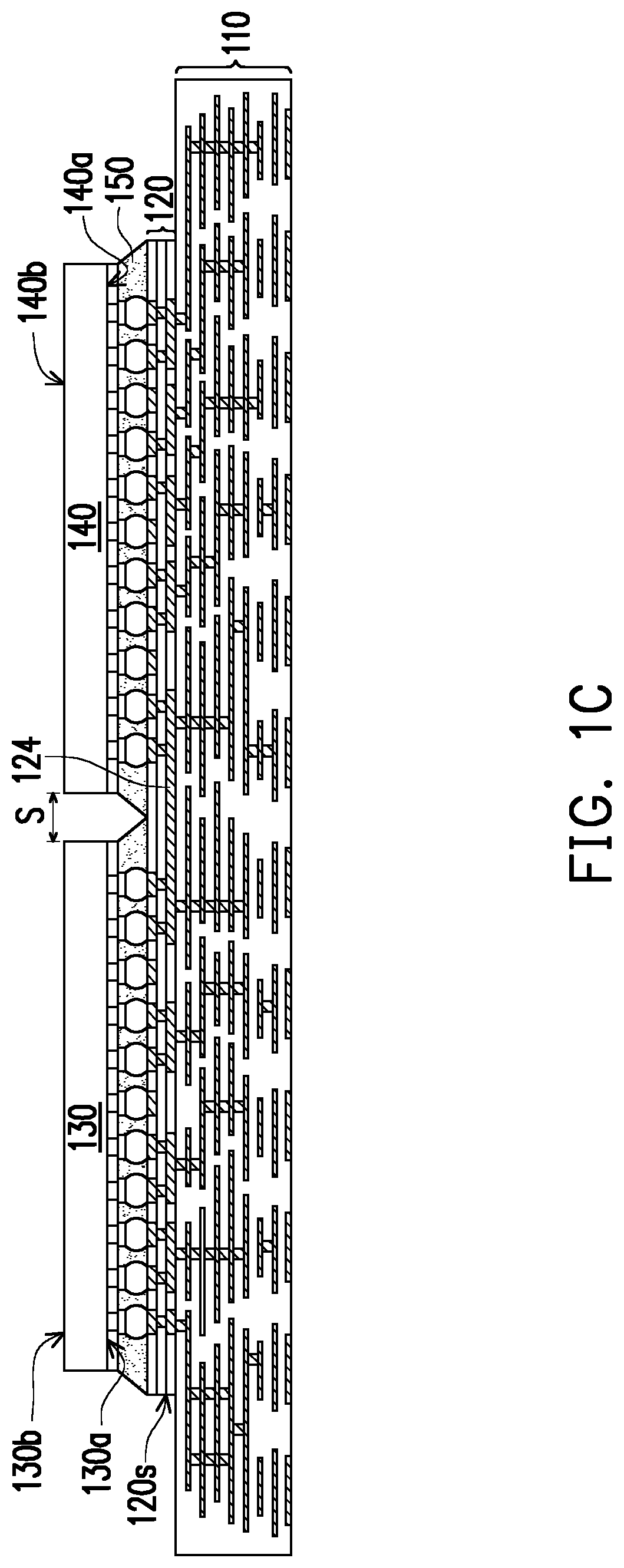
[0018]FIG. 1A to FIG. 1D are partial cross-sectional views showing a partial manufacturing method of a semiconductor package stru...


PUM


Abstract

A semiconductor package structure including a circuit substrate, a redistribution layer, and at least two dies is provided. The circuit substrate has a first surface and a second surface opposite the first surface. The redistribution layer is located on the first surface. The redistribution layer is electrically connected to the circuit substrate. The spacing of the opposing sidewalls of the redistribution layer is less than the spacing of the opposing sidewalls of the circuit substrate. The redistribution layer is directly in contact with the circuit substrate. At least two dies are disposed on the redistribution layer. Each of the at least two dies has an active surface facing the circuit substrate. One of the at least two dies is electrically connected to the other of the at least two dies by the redistribution layer. A manufacturing method of a semiconductor package structure is also provided.

Description

CROSS-REFERENCE TO RELATED APPLICATION[0001]This application claims the priority benefit of Taiwan application serial no. 108128494, filed on Aug. 12, 2019. The entirety of the above-mentioned patent application is hereby incorporated by reference herein and made a part of this specification.BACKGROUNDTechnical Field[0002]The present invention is related to a package structure and a manufacturing method thereof, and more particularly to a semiconductor package structure and a manufacturing method thereof.Description of Related Art[0003]For electronic products to achieve a compact design, the semiconductor packaging technology is also progressing to develop products that meet the requirements of small size, light weight, high density, and having high competitiveness in the market. In terms of a multi-function semiconductor package, how to enhance the electrical capability and / or performance of the semiconductor package structure while miniaturizing the semiconductor package structure...

Claims


Application Information

Patent Timeline
IPC IPC(8): H01L23/538H01L25/065H01L23/00H01L23/31H01L23/58H01L21/48H01L25/00
CPCH01L23/5386H01L2224/92125H01L24/32H01L23/3128H01L23/585H01L21/4857H01L25/50H01L23/5385H01L24/16H01L24/73H01L24/81H01L24/83H01L24/92H01L21/4853H01L2224/16227H01L2224/13025H01L24/13H01L2224/32225H01L2224/73204H01L25/0655H01L23/3107H01L24/02H01L21/4846H01L23/5389H01L2224/0233H01L23/562H01L23/055H01L23/49816H01L23/5383H01L2924/15311H01L2924/16251H01L2924/15192H01L2924/3511H01L2224/32058H01L2924/181H01L2924/16152H01L2224/83102H01L2224/2929H01L2224/29386H01L24/29H01L2224/83486H01L2224/81447H01L2224/8349H01L2224/81455H01L2224/81424H01L2224/13099H01L2224/2919H01L2224/16225H01L2924/00H01L2924/00014H01L2924/05442H01L2924/059H01L2924/05042H01L2924/04642H01L2924/07025
Inventor TSAI, PEI-CHUNHSU, HUNG-HSINCHANG CHIEN, SHANG-YULIN, NAN-CHUN
Owner POWERTECH TECHNOLOGY
Why Eureka
Try Eureka