Low-noise active-pixel sensor for imaging arrays with high speed row reset

a low-noise active-pixel sensor and imaging array technology, applied in the field of low-noise mos-based imagers, can solve the problems of fundamentally inferior temporal s/n performance of competing ccd imagers, imagers that are inferior to emerging charge coupled devices, and charge-amplification means that are not generally practical for on-chip implementation

Inactive Publication Date: 2003-03-11
RE SECURED NETWORKS LLC +2
View PDF33 Cites 116 Cited by
  • Summary
  • Abstract
  • Description
  • Claims
  • Application Information

AI Technical Summary

Problems solved by technology

Since such charge-amplification means were not generally practical for on-chip implementation in early MOS imaging sensors, alternative means compatible with NMOS technology were used.
Though these imagers were inferior to the emerging charge coupled device (CCD) imagers available at the time, similar MOS imagers are still being offered commercially.
Though much progress has been made in developing passive-pixel imagers, their temporal S / N performance is fundamentally inferior to competing CCD imagers because the bus capacitance translates to read noise of .apprxeq.100 e-.
These MOS imagers had adequate sensitivity, but their pixel pitch was too large at about 13 .mu.m.
All such proposals still offer inadequate performance.
U.S. Pat. No. 5,043,820 offers a method for injecting charge to reduce offset errors, but not with adequate accuracy and resolution to be useful for competing with CCDs.
Furthermore, these and other similar approaches which require 3-4 transistors in the pixel (at least one of which is relatively large to minimize amplifier 1 / f noise) in addition to the photodiode, also require off-chip signal processing for best S / N performance because none addresses the dominant source of temporal noise, namely the reset or "KTC" noise.
Adding the memory element to each pixel compromises the pixel optical fill factor or often requires circuit elements not strictly compatible with standard CMOS processes.
One alternative--adding the memory cell to the integrated circuit--greatly adds to the chip area and associated fabrication cost or increases vulnerability to blooming and lag.
The drawbacks of various prior art approaches are intractable because they increase imager cost.
For example, the '515 patent approach adds several transistors to each pixel and several million transistors to each imager thereby reducing production yield.
Ackland addresses the image lag issues associated with the intra-pixel charge transfer means but still requires a non-standard CMOS process.
Chi's implementation incurs reset noise and compromises spectral response at longer wavelengths by putting the photodiode in an n-well.
Many current systems require either expensive off-chip memory and signal processing or alternative APS schemes which attempt to mimic charge-coupled device technology to achieve low noise.
The latter schemes are typically not directly manufacturable using standard CMOS processes.
This requirement compromises the optical fill factor, but to a much smaller degree than if an optimally sized CDS capacitor were used instead.

Method used


Image

  • Low-noise active-pixel sensor for imaging arrays with high speed row reset
  • Low-noise active-pixel sensor for imaging arrays with high speed row reset
  • Low-noise active-pixel sensor for imaging arrays with high speed row reset

Examples


Embodiment Construction

The following description is provided to enable any person skilled in the art to make and use the invention and sets forth the best modes contemplated by the inventors of carrying out their invention. Various modifications, however, will remain readily apparent to those skilled in the art.

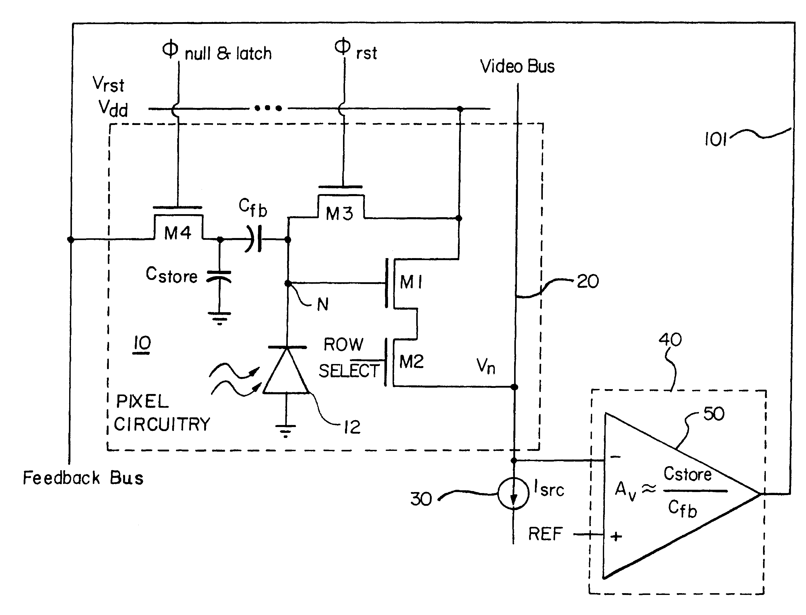
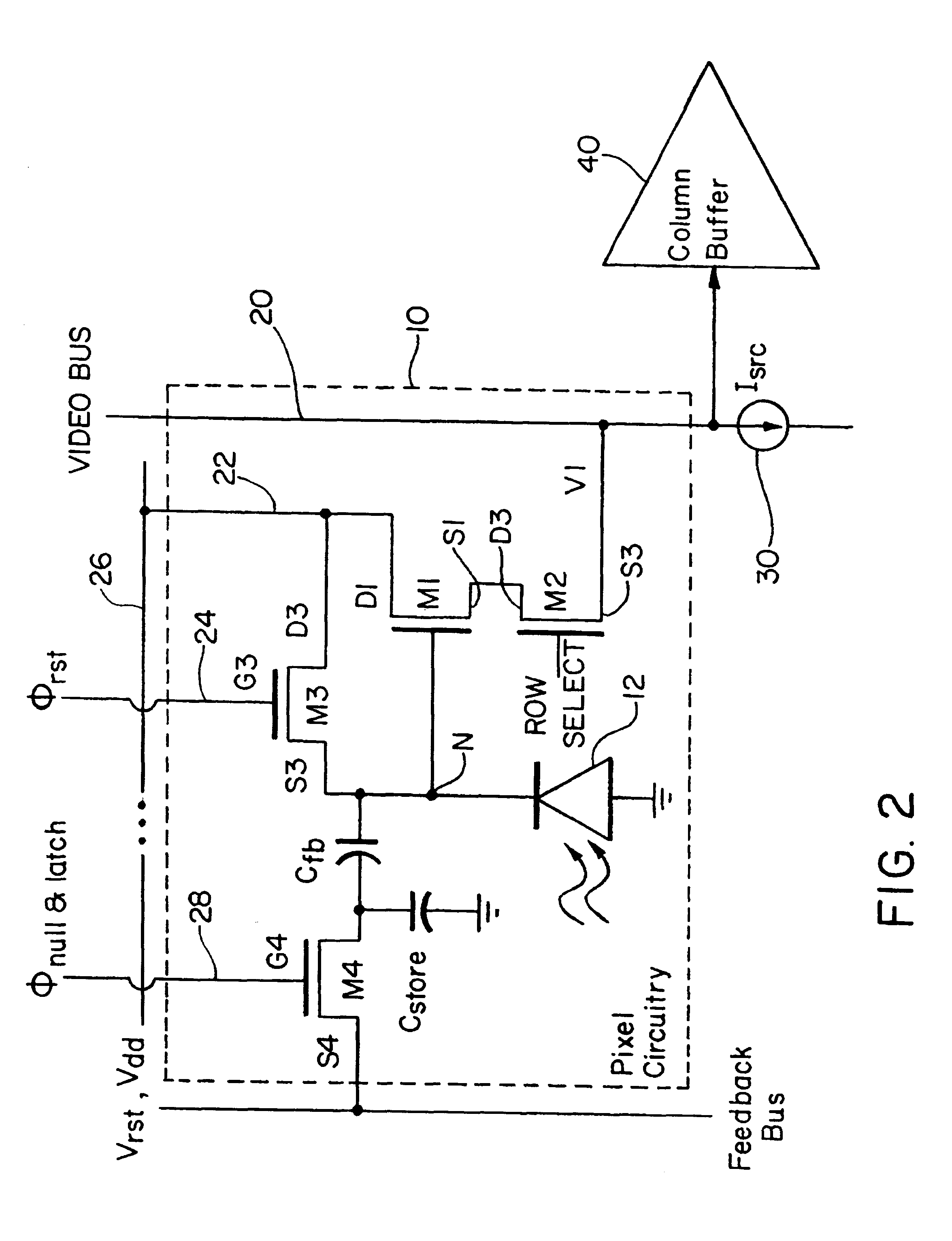
Visible imaging systems implemented in CMOS have the potential for significant reductions in cost and power requirements in components such as image sensors, drive electronics, and output signal conditioning electronics. An objective is a video camera that can be configured as a single CMOS integrated circuit supported by only an oscillator and a battery. Such a CMOS imaging system requires lower voltages and dissipates much less power than a CCD-based system. These improvements translate into smaller camera size, longer battery life, and applicability to many new products.

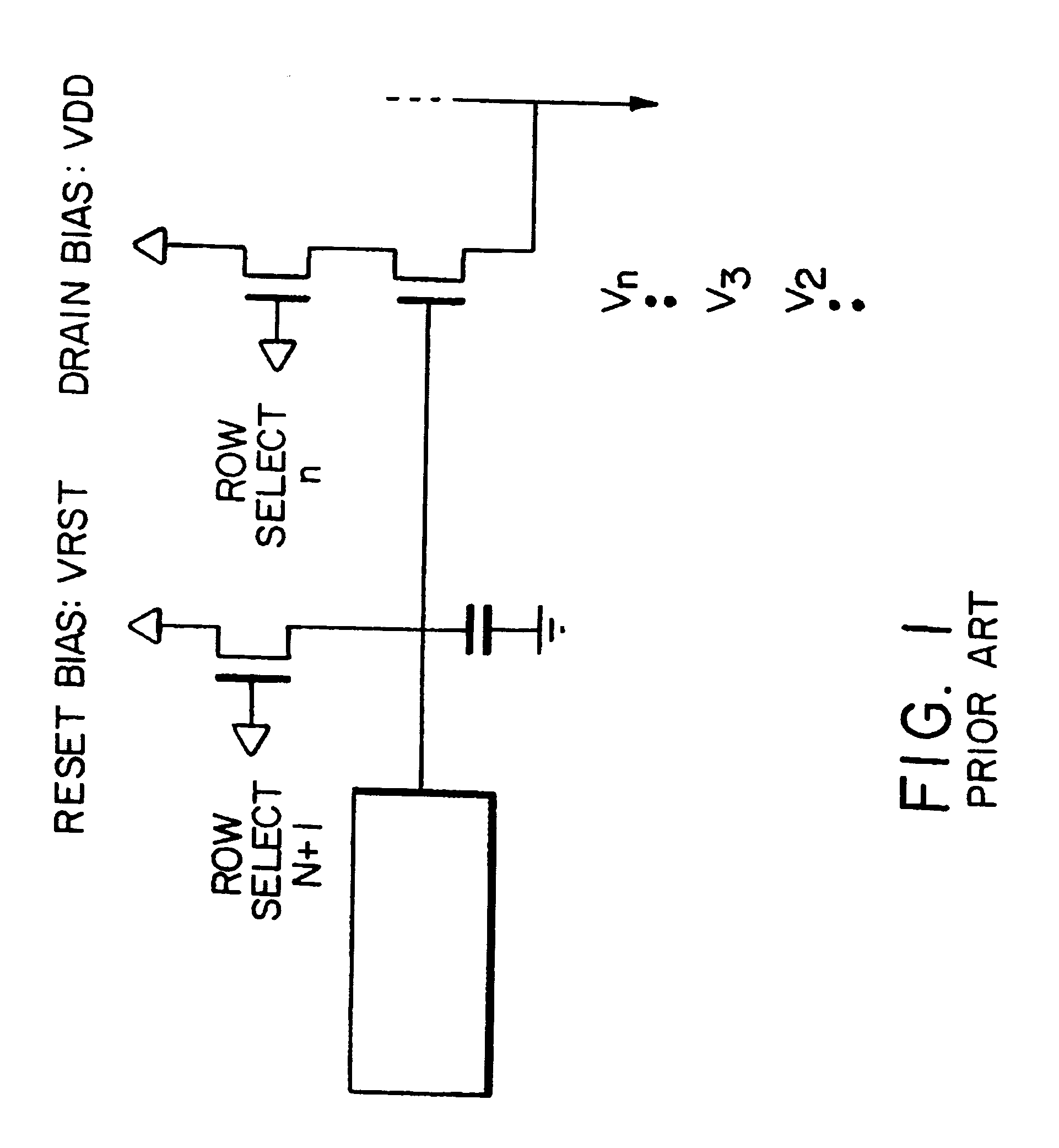
Because of the advantages offered by CMOS visible imagers, there have been ongoing -efforts to develop active-pixel sensor (APS...


PUM


Abstract

An imager pixel including a photodetector, a first MOS transistor functioning as the driver of a source follower amplifier during signal readout, a second MOS transistor serving as a pixel readout transistor, a third MOS transistor serving as a photodetector reset transistor, and a reset noise cancellation circuit including a fourth MOS transistor, first and second capacitances, and an amplifier having a gain which is the inverse of the ratio of the first to the second capacitance.

Description

1. Field of the InventionThe present invention relates to electronic imaging devices and, in particular, to low-noise MOS-based imagers having minimal analog components in each pixel. The invention provides both a method and apparatus for significantly improving cancellation of reset noise in an MOS active pixel sensor (APS).2. Description of Related ArtThe prior art describes many alternatives to CCD sensors for generating video or still images. The various schemes can be grouped into two basic classes, depending upon whether signal amplification is performed at each pixel or in support circuits. In the passive-pixel sensor, pixel simplicity and optical fill factor are maximized. Active-pixel sensors (APS's) include an amplifier at each pixel site to instead optimize signal transfer and sensitivity.The simplest passive pixel comprises a photodiode and an access transistor wherein the photo-generated charge is passively transferred from each pixel to downstream circuits. The integra...

Claims


Application Information

Patent Timeline
Patent Type & Authority Patents(United States)
IPC IPC(8): H04N3/15
CPCH03F3/087H04N5/378H04N5/37452H04N5/363H04N25/65H04N25/771H04N25/75
Inventor KOZLOWSKI, LESTER J.STANDLEY, DAVID L.
Owner RE SECURED NETWORKS LLC
Why Eureka
Try Eureka