Matrix-type display device
a display device and matrix-type technology, applied in the field of matrix-type display devices, can solve the problems of inability to ignore the occurrence of vertical offsets in the image, the degraded quality of the displayed moving image, and the usual appearance of the image, so as to improve the display of moving images
- Summary
- Abstract
- Description
- Claims
- Application Information
AI Technical Summary
Benefits of technology
Problems solved by technology
Method used
Image

Examples
first embodiment
1. First Embodiment
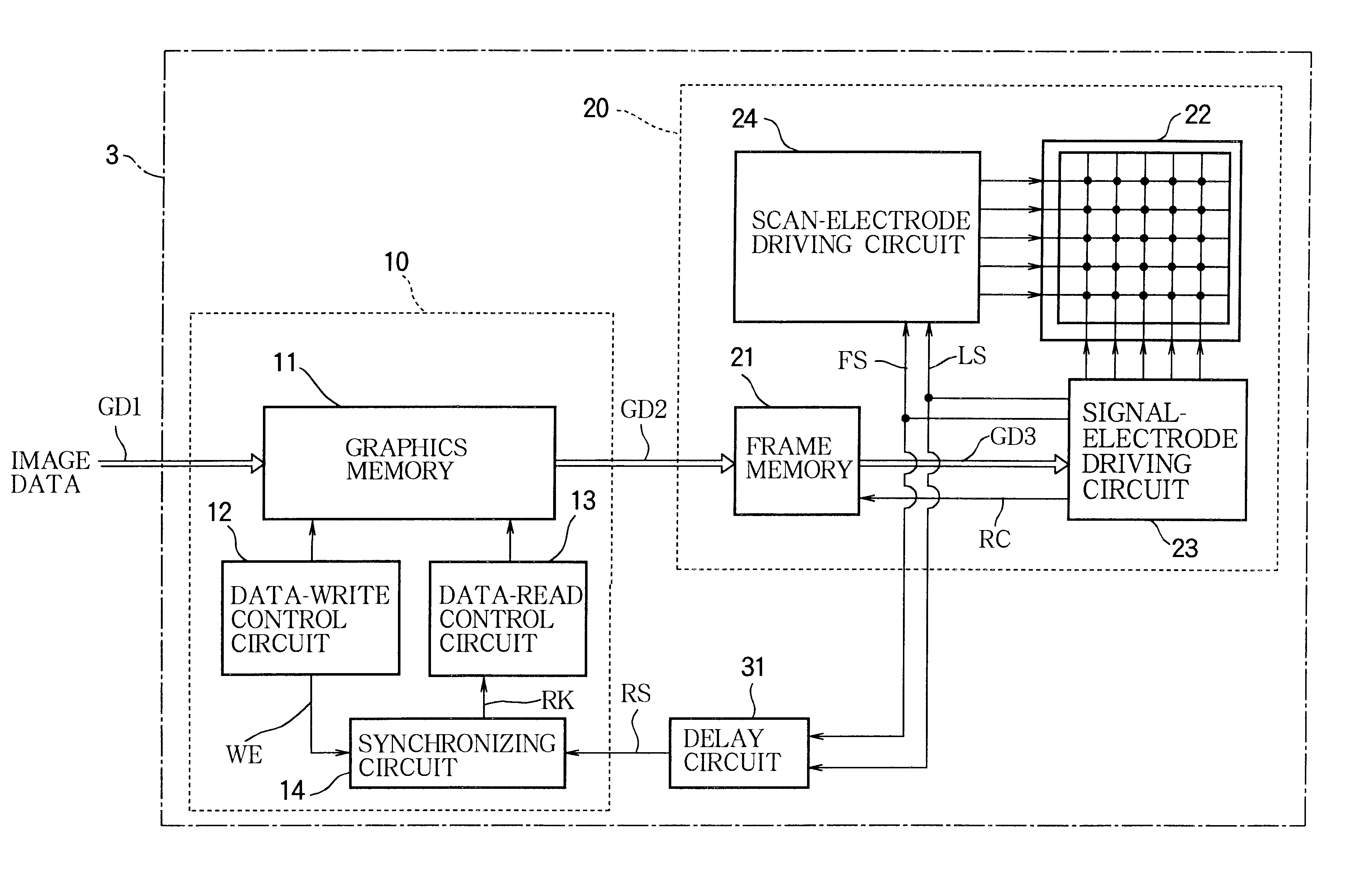
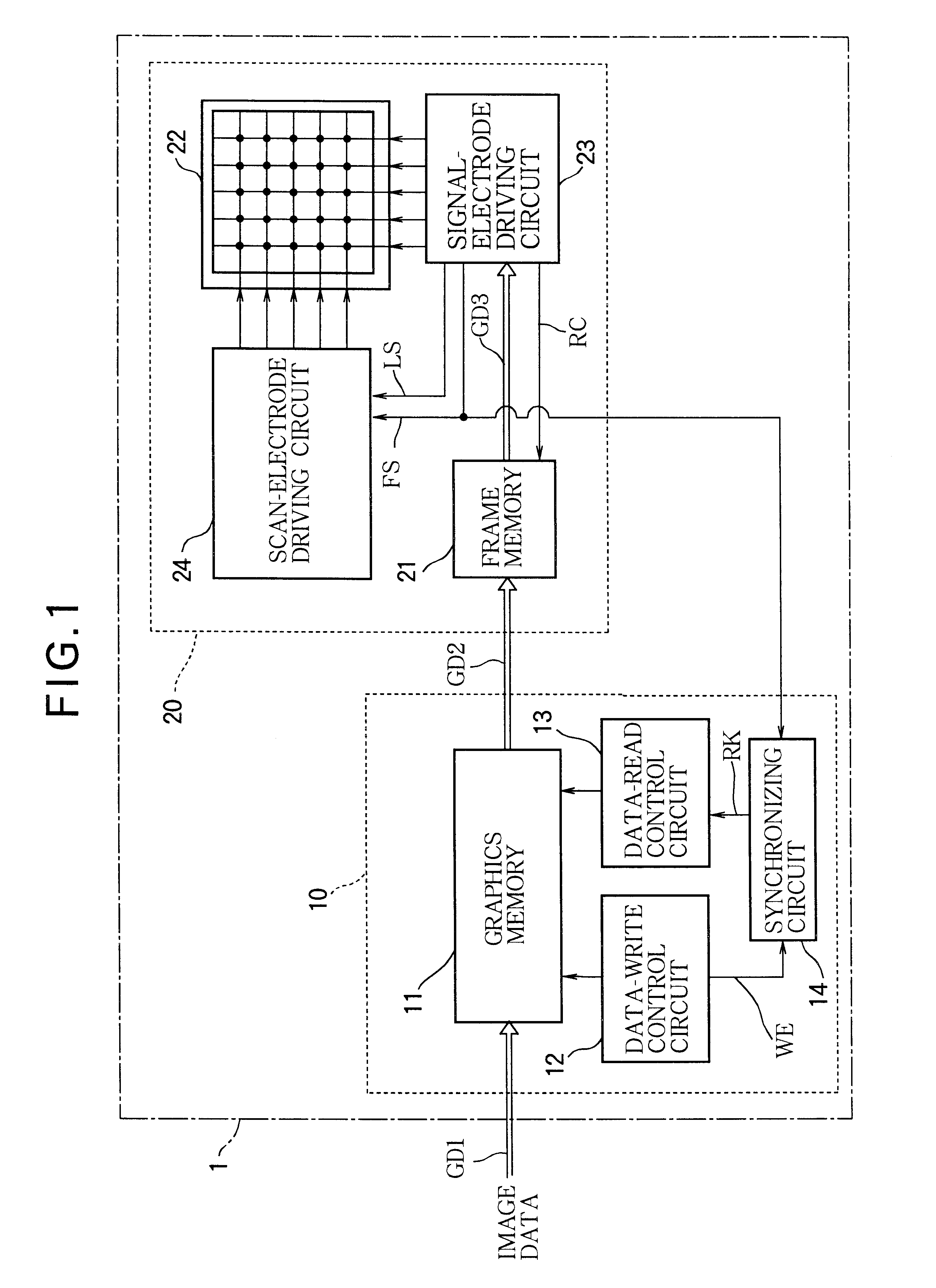
FIG. 1 is a drawing showing a first matrix-type display device embodying the present invention.
The principal way in which the matrix-type display device 1 of FIG. 1 differs from the matrix-type display device 9 of FIG. 9 is that, in the input control unit 10, there is a synchronizing circuit 14 that outputs a read-start signal to the data-read control circuit 13 in synchronization with the frame synchronization signal FS output from the signal-electrode driving circuit 23 in the display-panel module 20. Concomitant with the addition of the above synchronizing circuit 14, the data-write control circuit 12 is adapted to be able to output a write-end signal WE to the synchronizing circuit 14, and the signal-electrode driving circuit 23 is adapted to be able to send the frame synchronization signal both to the scan-electrode driving circuit 24 and the synchronizing circuit 14. As for the rest of the structure, it is the same as in the conventional matrix-type display ...
second embodiment
2. Second Embodiment
The first embodiment avoided the switching of the image to a newly written image midway through the image data GD3 read from the frame memory 21 by synchronizing the timing of the start of the transfer of image data GD2 from the graphics memory 11 to the frame memory 21 with the frame synchronization signal FS, with a delay time DT1 from the frame synchronization signal FS to the reading of the image data GD3 from the frame memory 21. If the delay time DT1 is increased, however, then the timing of the end of the transfer of image data GD2 approaches the timing of the end of the reading of the image data GD3 of frame (n+1) in FIG. 4, and if the timing of the end of the transfer of image data GD2 overtakes the timing of the end of the reading of image data GD3, the possibility again arises that the image displayed on the matrix display panel 22 will switch over, partway through one frame, to the next frame.
The second embodiment, described below, adjusts the delay t...
third embodiment
The third embodiment is therefore structured to input the line synchronization signal LS as the clock signal of the delay circuit 31, as shown in FIG. 8. A signal obtained by delaying the frame synchronization signal FS by a preset number of pulses of the line synchronization signal LS can then be output from the delay circuit 31 as the read synchronization signal RS. In this case, the amount by which the read synchronization signal RS is delayed from the frame synchronization signal FS does not vary, so the transfer of image data GD2 in synchronization with the read synchronization signal RS can be synchronized reliably with the timing t5 of the end of the reading of the image data GD3 of frame (n+1). Accordingly, the situation in which, midway through one frame of the image displayed on the matrix display panel 22, there is a switchover to the image of the next frame can be eliminated.
The third embodiment thus inputs the line synchronization signal LS, as well as the frame synchro...
PUM
 Abstract
Description
Claims
Application Information
 - R&D Engineer
- R&D Manager
- IP Professional
- Industry Leading Data Capabilities
- Powerful AI technology
- Patent DNA Extraction
Browse by: Latest US Patents, China's latest patents, Technical Efficacy Thesaurus, Application Domain, Technology Topic.
© 2024 PatSnap. All rights reserved.Legal|Privacy policy|Modern Slavery Act Transparency Statement|Sitemap