Information recording medium with SiO2-In2O3-SnO2-ZnS protective layer

Inactive Publication Date: 2005-02-08
HITACHI LTD
View PDF5 Cites 12 Cited by
  • Summary
  • Abstract
  • Description
  • Claims
  • Application Information

AI Technical Summary

Benefits of technology

Furthermore, as described in JP-A-2001-266408, when the first protective layer is as thick as 50 nm or more, a tact time of sputtering is long due to time-consuming film formation. Thus, there occurs a problem that mass productivity is low. Here, thinning of the first protective layer is conceivable, however, if the first protective layer is thin, heat generated in the recording film in the numerous rewritings is transmitted to the substrate, thus causing a problem of likely deterioration in the substrate. An object of the present invention is to solve the foregoing problems and to provide an information recording medium, in which the stress between the laminated films and the substrate is small, material costs and mass productivity are excellent and the substrate is unlikely to deteriorate in the numerous rewritings.
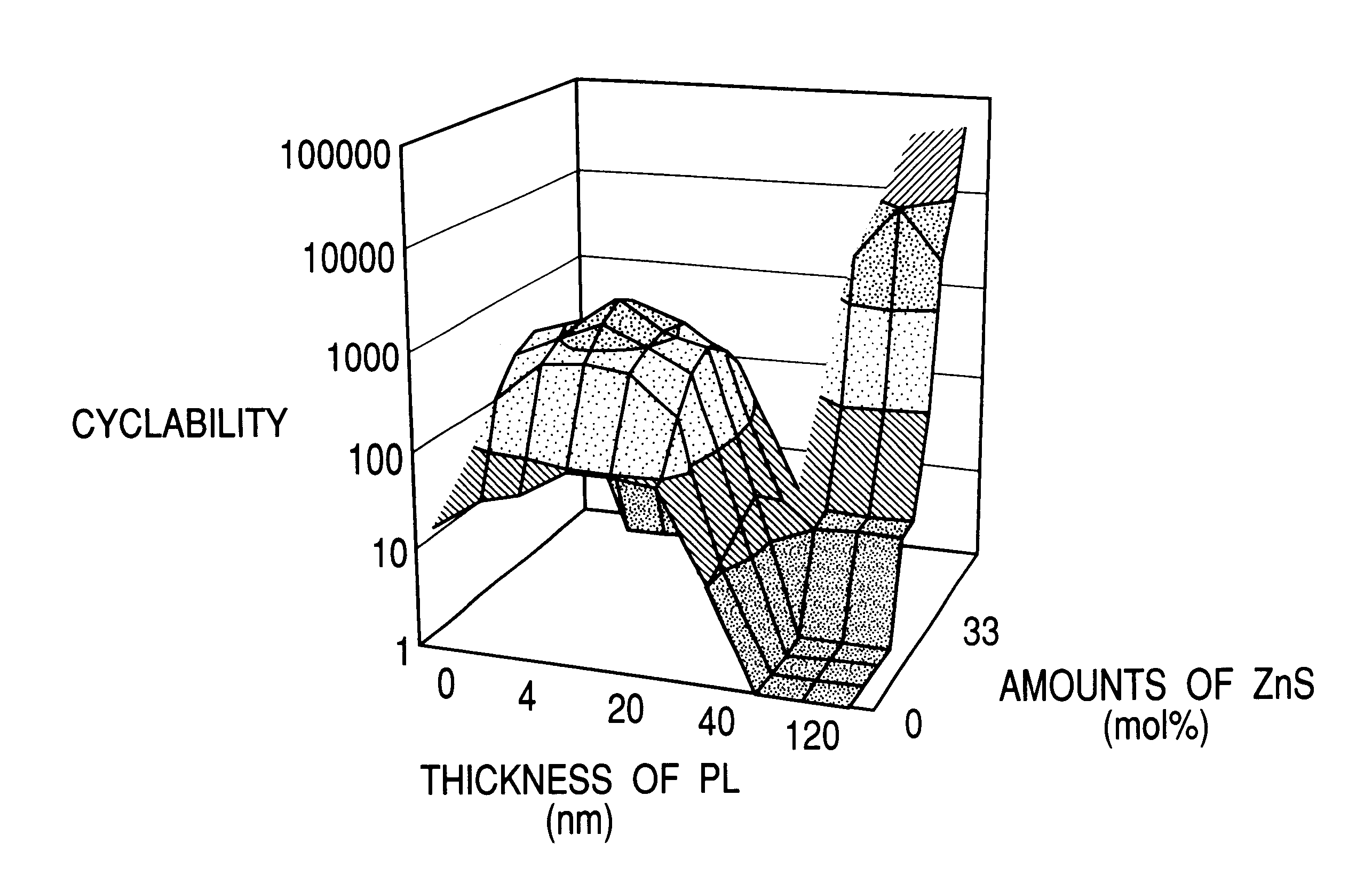
In order to solve the foregoing problems, in the information recording medium of the present invention, the following countermeasure is used. Specifically, the film thickness of the first protective layer is set as thin as in the range of 2 nm to 25 nm, 95 atomic % or more of a material of the first protective layer is composed of SiO2—In2O3—SnO2—ZnS, and a ZnS amount in the first protective layer is set in the range of 4 mol % to 33 mol %. Consequently, the number of possible rewrites becomes 300 times or more, leading to a combined effect in mass productivity and rewriting properties.
Furthermore, it is more preferable that the film thickness of the first protective layer is set in the range of 4 nm to 20 nm and the ZnS amount in the first protective layer is set in the range of 6 mol % to 30 mol %. Consequently, the number of possible rewrites becomes 1000 times or more, leading to a combined effect in mass productivity and rewriting properties.
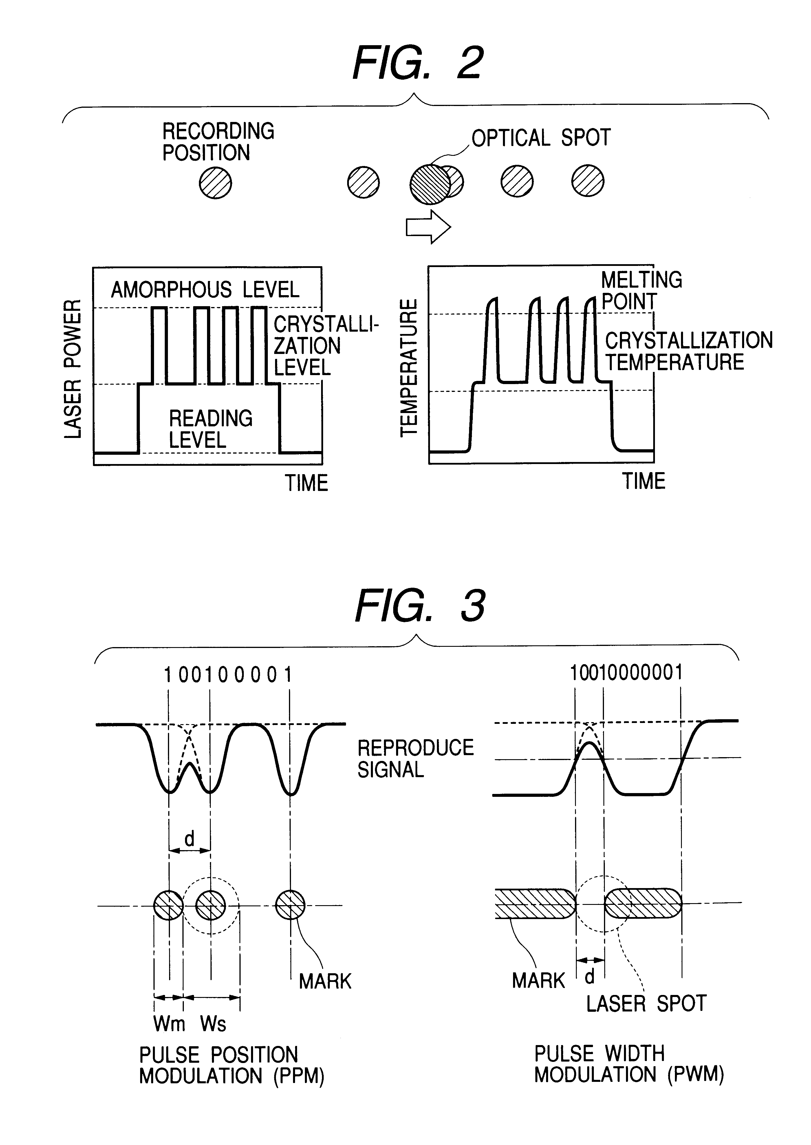
In the DVD-RAM and a DVD-RW (Digital Versatile Disk-Rewritable), a mark edge recording method is adopted, which can realize a high-density recording. In the mark edge recording, positions of both edges of a recording mark formed on a recording film are made to correspond to digital data of 1. Accordingly, a length of a shortest recording mark is made to correspond not to one reference clock but to two to three reference clocks, thus enabling the high-density recording. In the DVD-RAM, an 8-16 modulation system is adopted, and the length of the recording mark is made to correspond to three reference clocks. As shown in a comparison of FIG. 3, compared to a mark position recording in which a center position of a circle recording mark is made to correspond to the digital data of 1, the mark edge recording method has an advantage of capability of performing the high-density recording without reducing the recording mark to an extremely small size. However, for the recording medium it is required that deformation in a shape of the recording mark is extremely small. In FIG. 3, Ws is a diameter of a beam spot, Wm is a mark length, and d is a resolution.
As described above, one layer has a plurality of roles, and functions of the respective layers are intricately intertwined with each other. The stress reduction by the thinning of the first protective layer prevents groove deformation, thus contributing to the making of the track pitch narrower. Therefore, the optimal selection of a combination of laminated films and the selection of film thickness are extremely important in offering the technical advantages.

Problems solved by technology

Thus, in the case of performing push-pull tracking for the tracking grooves, address data in the pre-format portion are unreadable.
When a tracking offset is corrected so as to set the recording track in a normal position with respect to the pre-format portion, there occurs a problem that an offset in a recording area partially deletes data of an adjacent track.
Furthermore, as described in JP-A-2001-266408, when the first protective layer is as thick as 50 nm or more, a tact time of sputtering is long due to time-consuming film formation.
Thus, there occurs a problem that mass productivity is low.
Here, thinning of the first protective layer is conceivable, however, if the first protective layer is thin, heat generated in the recording film in the numerous rewritings is transmitted to the substrate, thus causing a problem of likely deterioration in the substrate.

Method used


Image

  • Information recording medium with SiO2-In2O3-SnO2-ZnS protective layer
  • Information recording medium with SiO2-In2O3-SnO2-ZnS protective layer
  • Information recording medium with SiO2-In2O3-SnO2-ZnS protective layer

Examples


embodiment 1

[Embodiment 1]

(Constitution of an Information Recording Medium of the Present Invention and a Manufacturing Method Thereof)

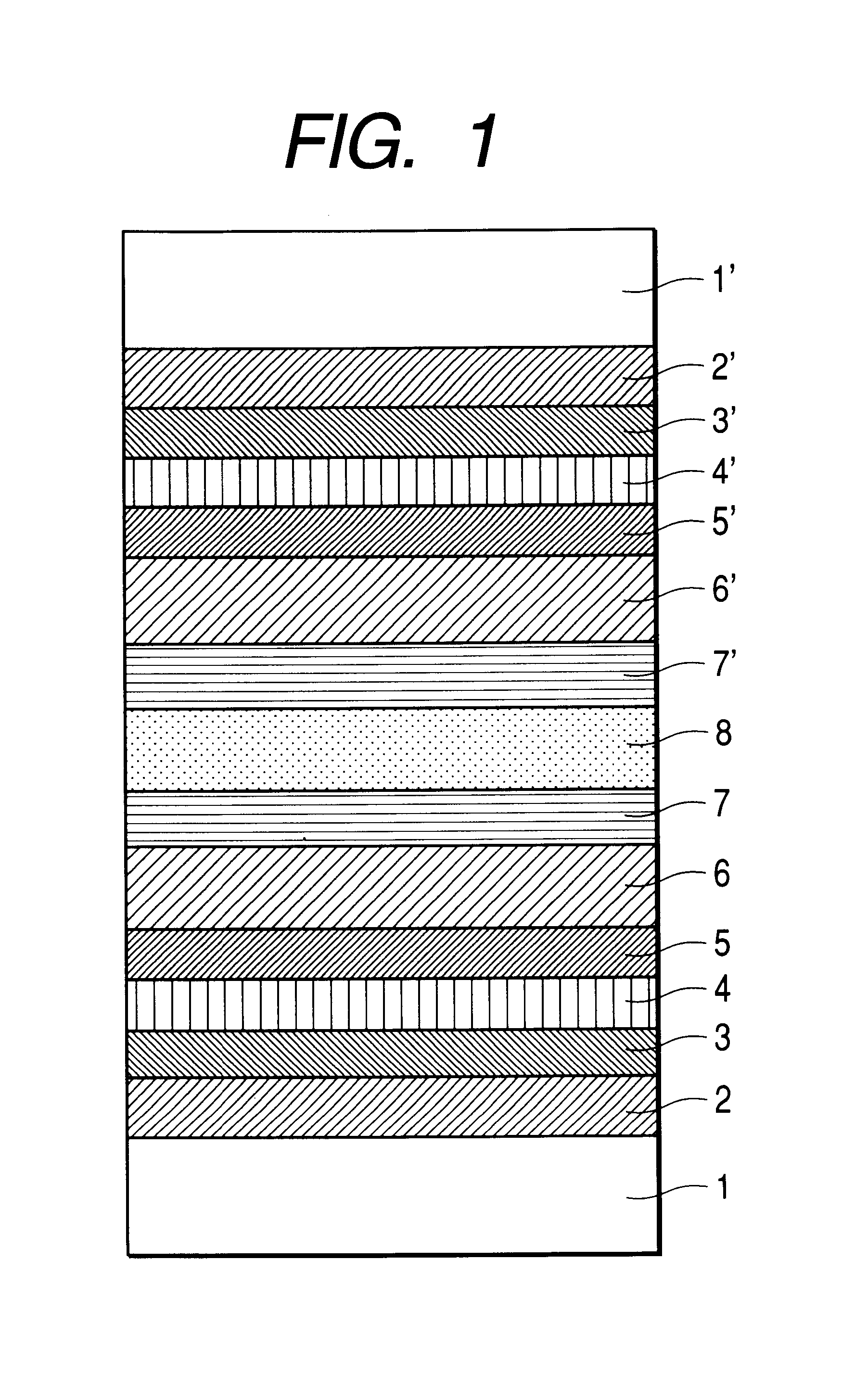
FIG. 1 is a view showing a cross-section structure of a disk-shaped information recording medium according to a first embodiment of the present invention. The above medium is manufactured as described below.

First, on a polycarbonate substrate 1 with a diameter of 12 cm and a thickness of 0.6 mm, which has tracking grooves of land / groove recording at a track pitch of 0.615 micron on its surface and has pit rows expressing address information and the like at a position shifted from a track center, that is, approximately on an extension of a boundary line of a land and a groove, a first protective layer 2 made of (SiO2)60((In2O3)90(SnO2)10)25(ZnS)15 with a film thickness of 8 nm. Next, a lower interface layer 3 made of a Cr2O3 film is formed with a film thickness of 2 nm. Subsequently, the followings are sequentially formed, including: a recording film 4 made of Ge...

embodiment 2

[Embodiment 2]

COMPARATIVE EXAMPLE 1

A disk (comparative example 1), which is different from the disk of the embodiment 1 only in the first protective layer, is prepared, and the tact is compared therebetween by a similar method to the embodiment 1. Then, the following result is obtained.

(Production Tact)

As to the information recording medium of the comparative example 1, when six layers are formed by use of a film formation device, the lamination tact is 40 seconds, which is decided depending on a sputtering rate of a material constituting each of the layers and a film thickness of the laminated layer.

TABLE 4FilmLaminationChamber numberthicknesstime(formed layer)Constitution material(nm)(s)1 (First protec-(ZnS)80(SiO2)2012040tive layer)2 (Interface layer)Cr2O3233 (Recording film)Ge7Sb2Te41064 (Second protec-SnO2336tive layer)5 (AbsorptionCr90(Cr2O3)10349control layer)6 (Reflective layer)Al609

In a film formation device having seven chambers or more, the tact can be further shortened. ...

embodiment 3

[Embodiment 3]

COMPARATIVE EXAMPLE 2

A disk (comparative example 2), which is different from the disk of the embodiment 1 only in the material of the first protective layer, is prepared, and a jitter in the numerous rewritings is measured by use of a similar method to the embodiment 1. Then, as shown in FIG. 7, the jitter increases to 13% or more after overwrites of more than 100 times.

As to the first protective layer according to the comparative example 2, a first protective layer 2 made of (SiO2)60((In2O3)90(SnO2)10)40 is formed with a film thickness of 8 nm. As to a method for forming the film, sputtering is performed in an Ar gas atmosphere.


PUM


Abstract

In an information recording medium, a first protective layer, a recording film, a second protective layer and a reflective layer are provided on a substrate sequentially from a side where light is irradiated, the first protective layer having a film thickness of 2 nm to 25 nm. 95 atomic % or more of a material of the first protective layer is SiO2—In2O3—SnO2—ZnS, and a ZnS amount in the first protective layer is in the range of 4 mol % to 33 mol %.

Description

BACKGROUND OF THE INVENTIONThe present invention relates to an information recording medium used in an optical disk.There are known various principles of recording information on a thin film (recording film) by laser beam irradiation. Among them, a principle utilizing a change in atomic arrangement by the laser beam irradiation, such as a phase change (also called a phase transition or a phase transformation) of a film material, is hardly subjected to deformation of the thin film, thus having an advantage of obtaining an information recording medium having a double-sided disk structure obtained by sticking two disk members together directly.Generally, such an information recording medium has a constitution in which a first protective layer, a recording film of GeSbTe series and the like, an upper protective layer and a reflective layer are provided on a substrate. In JP-A-2001-266408, description is made concerning that (ZnS)60(SiO2)30C10 is used as a first protective layer and a fi...

Claims


Application Information

Patent Timeline
IPC IPC(8): B32B3/02G11B3/00G11B7/26G11B23/03G11B3/70G11B7/24G11B5/84G11B7/2403G11B7/241G11B7/243G11B7/2433G11B7/254G11B7/257G11B7/2578
CPCG11B7/2403G11B7/252G11B7/2578G11B7/2534G11B2007/25715G11B2007/24312G11B2007/24314G11B2007/24316G11B2007/2571G11B7/2585
InventorHIROTSUNE, AKEMITERAO, MOTOYASUANZAI, YUMIKO
OwnerHITACHI LTD