Method and apparatus for storing image information for multiple sampling operations in a digital pixel sensor

Active Publication Date: 2006-01-17
PIXIM
View PDF6 Cites 22 Cited by
  • Summary
  • Abstract
  • Description
  • Claims
  • Application Information

AI Technical Summary

Benefits of technology

[0011]The image information storage method of the present invention permits the size of the on-chip memory in a digital image sensor to be reduced while preserving the image r

Problems solved by technology

While this ADC approach requires fairly simple and robust circuits, it has the disadvantages of producing too much data and suffering from poor l

Method used


Image

  • Method and apparatus for storing image information for multiple sampling operations in a digital pixel sensor
  • Method and apparatus for storing image information for multiple sampling operations in a digital pixel sensor
  • Method and apparatus for storing image information for multiple sampling operations in a digital pixel sensor

Examples


Embodiment Construction

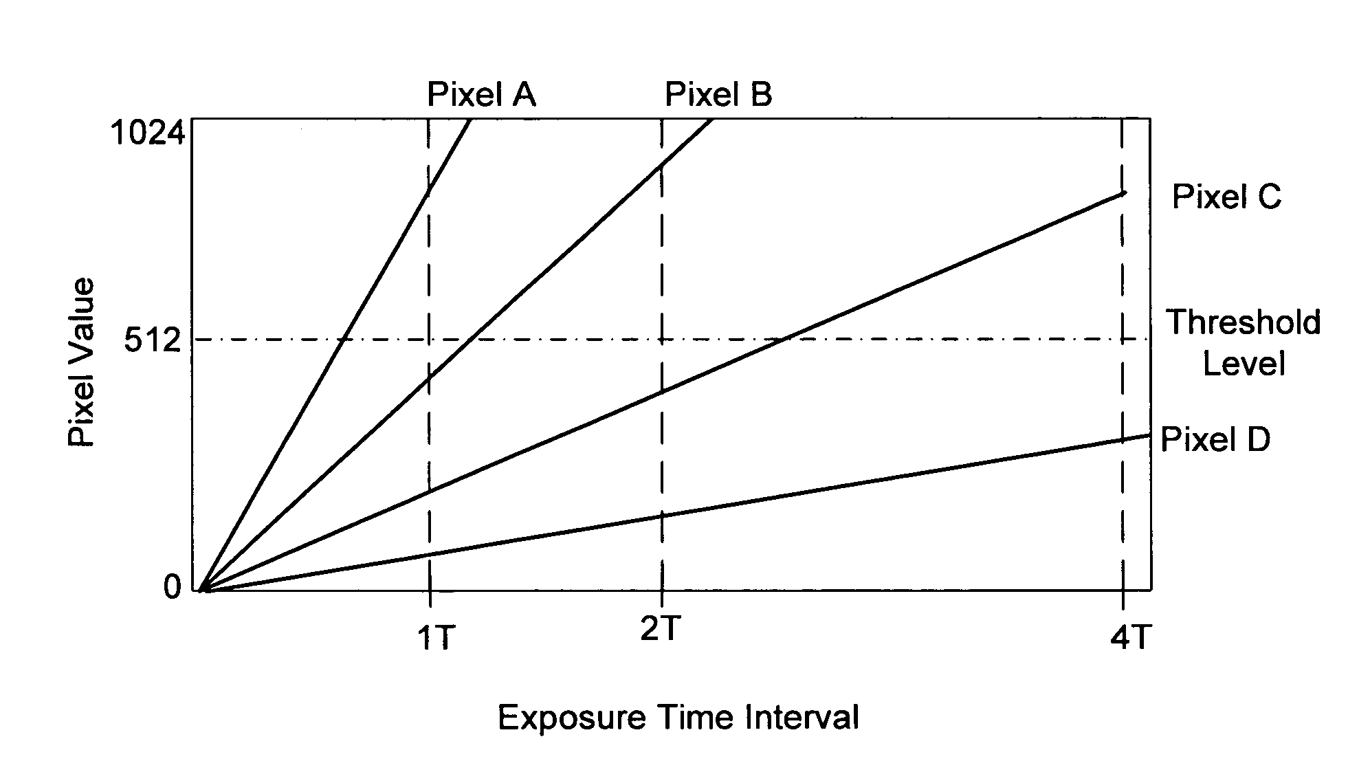
[0022]In accordance with the present invention, a method and apparatus for storing image information in a digital pixel sensor is provided for reducing the size of the memory needed to facilitate multiple sampling. The image information storage method of the present invention permits the size of the on-chip memory in a digital image sensor to be reduced while preserving the image resolution. By reducing the size of the on-chip memory, the present invention provides the benefits of reducing manufacturing cost and improving production yield.

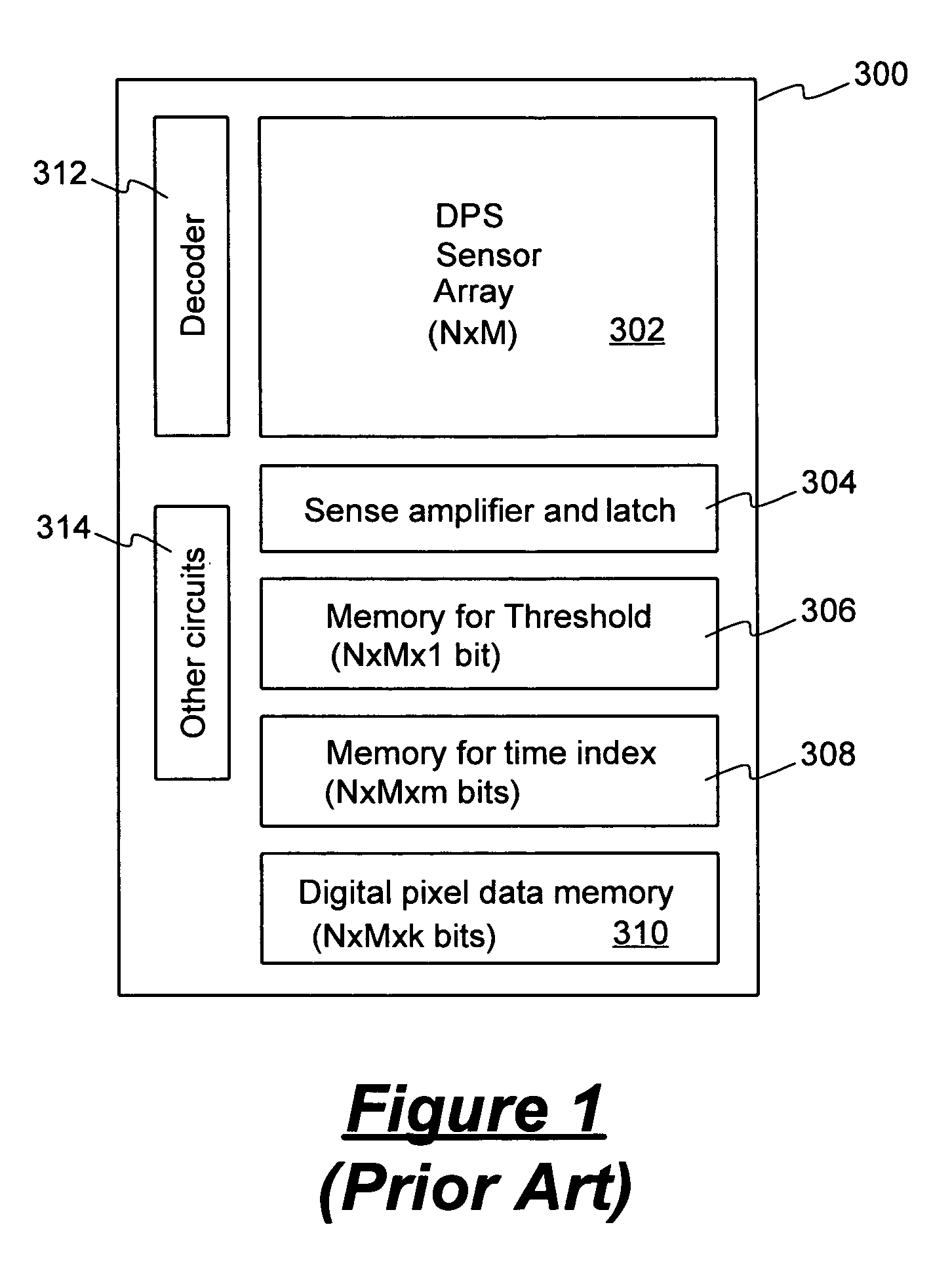
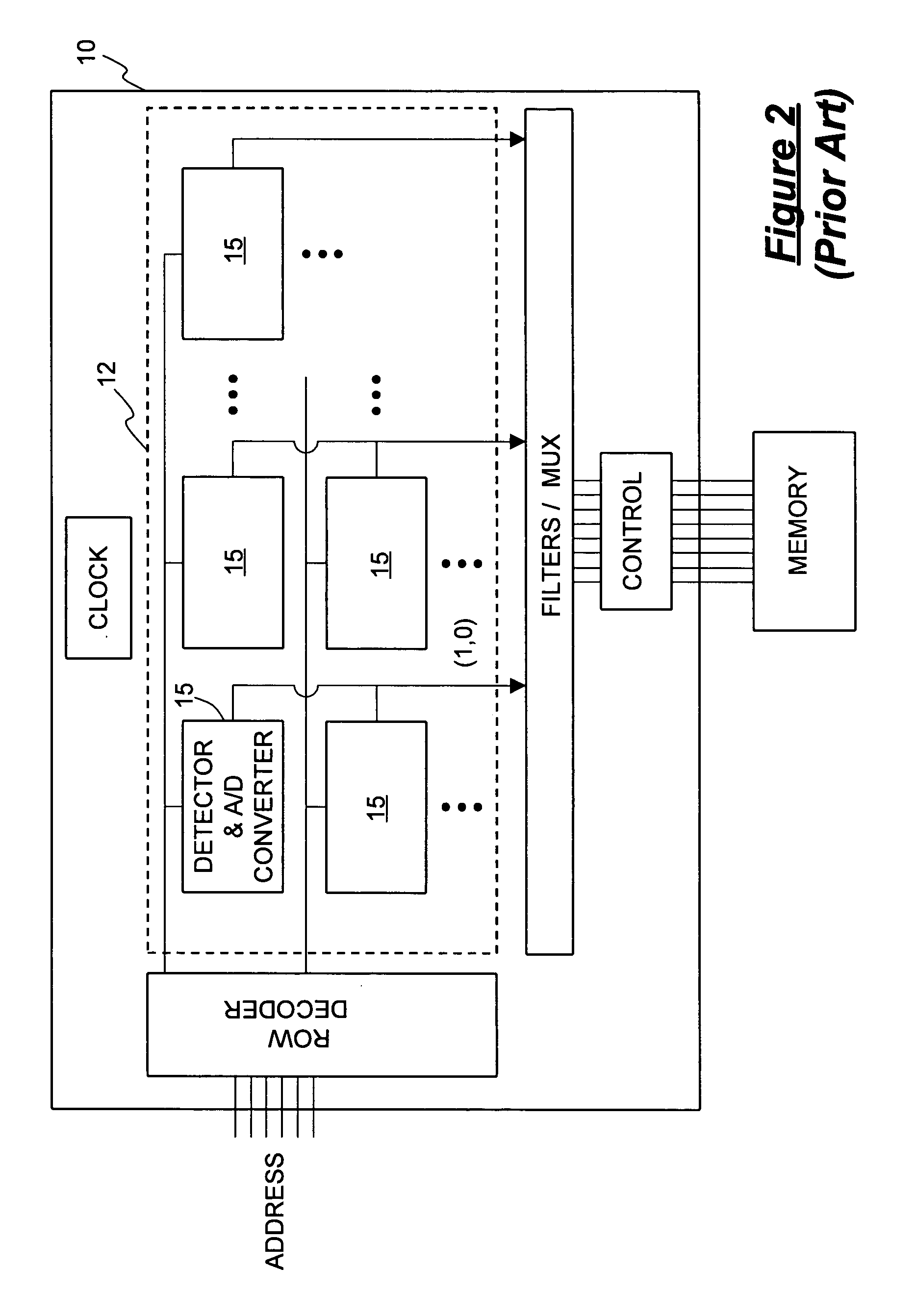
[0023]In the present description, a digital pixel sensor (DPS) array or a sensor array refers to a digital image sensor having an array of photodetectors where each photodetector produces a digital output signal. In one embodiment of the present invention, the DPS array implements the digital pixel sensor architecture illustrated in FIG. 2 and described in the aforementioned '425 patent. The DPS array of the '425 patent utilizes pixel level analog-...


PUM


Abstract

A method for storing image information in a digital pixel sensor is disclosed for reducing the size of the memory needed to facilitate multiple sampling. An image sensor includes a sensor array of pixel elements generating pixel data in k bits and a data memory for storing pixel data of each pixel element. In one embodiment, the data memory in the digital pixel sensor stores an m-bit time index value and the lower k−1 bits of the pixel data for pixel data exceeding the predetermined threshold level in all exposure times except the last. When pixel data in the last exposure time is captured, the data memory stores the time index value in less than m bits and stores the k-bit pixel data. The size of the data memory is minimized while preserving the image quality. The method of the present invention provides the benefits of reducing manufacturing cost and improving production yield.

Description

CROSS-REFERENCE TO RELATED APPLICATION[0001]The present application is related to concurrently filed and commonly assigned U.S. patent application bearing Ser. No. 09 / 823,843, entitled “Method And Apparatus for Companding Pixel Data in a Digital Pixel Sensor,” by Justin Reyneri and Benjamin P. Olding.FIELD OF THE INVENTION[0002]The invention relates image sensor systems, and in particular, the present invention relates to a method for storing image information when multiple sampling is used in a digital image sensor.BACKGROUND OF THE INVENTION[0003]A CMOS image sensor with pixel level analog-to-digital conversion is described in U.S. Pat. No. 5,461,425 of B. Fowler et al. (the '425 patent). Such an image sensor, referred to as a digital pixel sensor (DPS), provides a digital output signal at each pixel element representing the light intensity detected by that pixel element. The combination of a photodetector and an analog-to-digital (A / D) converter in an area image sensor helps enha...

Claims


Application Information

Patent Timeline
IPC IPC(8): H04N3/14H04N5/235
CPCH04N5/235H04N23/70
Inventor OLDING, BENJAMIN P.REYNERI, JUSTIN
Owner PIXIM
Why Eureka
Try Eureka