Giant magnetoresistance (GMR) read head with reactive-ion-etch defined read width and fabrication process
a read head and reactive ion etch technology, applied in nanoinformatics, instruments, record information storage, etc., can solve the problems of difficult to achieve a designed read width and the design read width cannot be easily achieved, so as to reduce the width of the read track, and reduce the side reading problem
- Summary
- Abstract
- Description
- Claims
- Application Information
AI Technical Summary
Benefits of technology
Problems solved by technology
Method used
Image

Examples
first embodiment
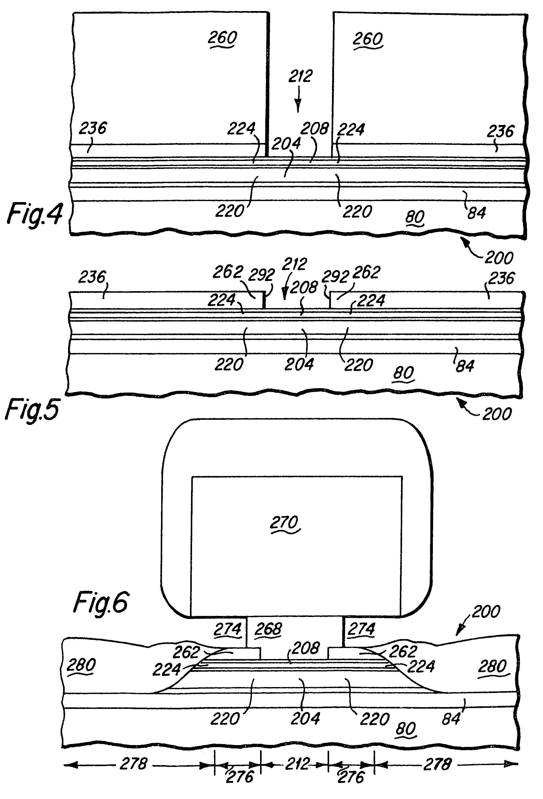
[0029]As depicted in FIGS. 4–7, and particularly FIG. 7, the GMR read head 200 of the present invention includes a GMR read sensor 204 and a LB stack 208 in a read region 212, outer portions 220 of the GMR read sensor, outer portions 224 of the LB stack and two spaced apart portions 262 of a first conductor layer 236 disposed in two sideways displaced overlay regions 276, and also includes a second conductor layer 280 disposed in two side regions 278. Particularly, the GMR read sensor 204 may include Al2O3(3) / NiCrFe(3) / NiFe(1) / PtMn(15) / CoFe(1.6) / Ru(0.8) / CoFe(1.8) / CuO(2.2) / CoFe(2) / Cu(0.6) / Ru(2.4) films, the LB stack 208 may include CoFe(3) / IrMn(6) / Ru(3) layers, and the first conductor layer 236 may be formed of a Ta(20) film. In the head fabrication process, a bottom shield layer 80 is fabricated upon a wafer substrate. An insulating bottom gap layer (G1) 84, the GMR read sensor 204, the LB stack 208, and the first conductor layer 236 are all sequentially deposited on a wafer. After ...
second embodiment
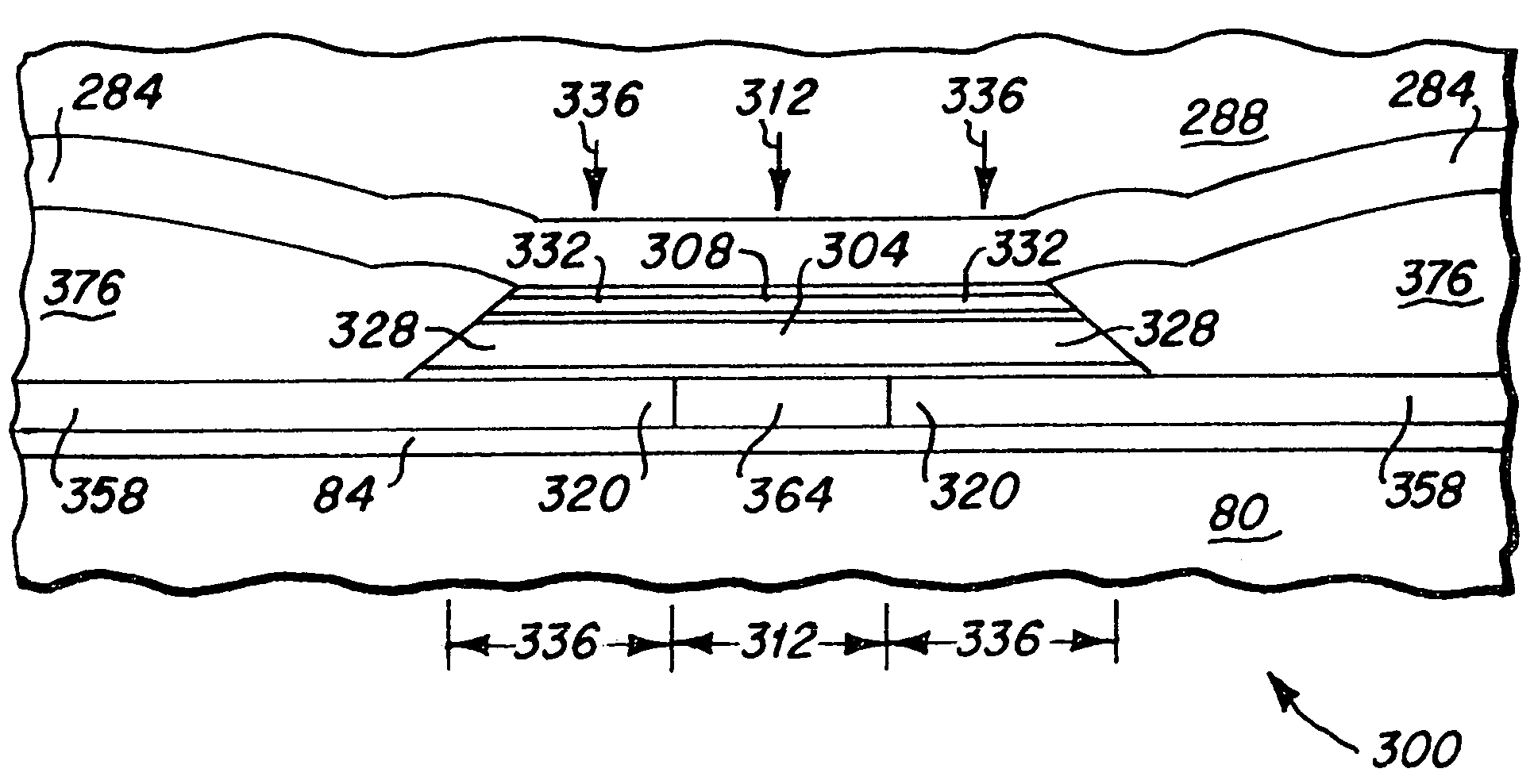
[0035]After these two anneals, bilayer photoresists 366 and 368 are applied, as shown in FIG. 10, and exposed in a photolithographic tool to mask the read and overlay regions, and then developed in a solvent to form an undercut 372. The multilayer films in the unmasked side region are removed by ion milling until the first conductor layer 358 is exposed, and a second conductor layer 376 that may include Ta(3) / Rh(80) / Ta(3) films is then deposited in the unmasked side regions. After this deposition, the bilayer photoresists are lifted off and the read head fabrication process continues as described above. After the completion of this read head fabrication process, the write head fabrication process starts. After the completion of the read / write head fabrication process, the sensor height is defined by lapping along the alignment mark. This second embodiment also possesses well defined read width and stability, and side writing is substantially eliminated.
PUM
| Property | Measurement | Unit |
|---|---|---|
| magnetization | aaaaa | aaaaa |
| critical thickness | aaaaa | aaaaa |
| electrically conducting | aaaaa | aaaaa |
Abstract
Description
Claims
Application Information
 - R&D Engineer
- R&D Manager
- IP Professional
- Industry Leading Data Capabilities
- Powerful AI technology
- Patent DNA Extraction
Browse by: Latest US Patents, China's latest patents, Technical Efficacy Thesaurus, Application Domain, Technology Topic.
© 2024 PatSnap. All rights reserved.Legal|Privacy policy|Modern Slavery Act Transparency Statement|Sitemap