

Method for forming a silicon nitride layer
a silicon nitride and layer technology, applied in the field of semiconductor technology, can solve the problems of difficult diffusion of nitrogen atoms in the ambient environment, and achieve the effect of increasing the capacity of the layer
- Summary
- Abstract
- Description
- Claims
- Application Information
AI Technical Summary
Benefits of technology
Problems solved by technology
Method used
Image

Examples
Embodiment Construction
Method of Forming a Silicon Nitride Layer
[0026]FIGS. 2a to 2d are cross-sections of a method of forming a silicon nitride layer of the invention.
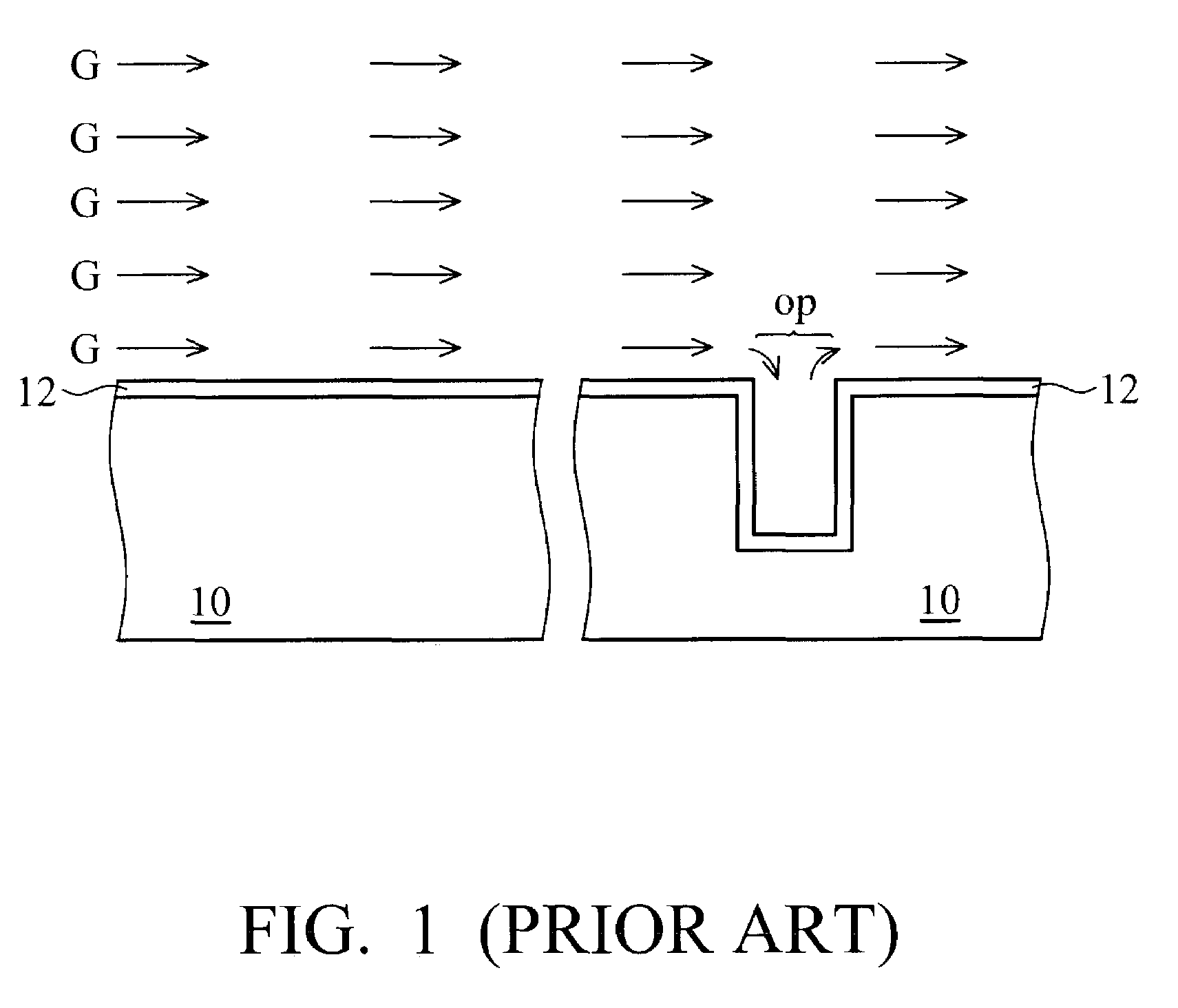
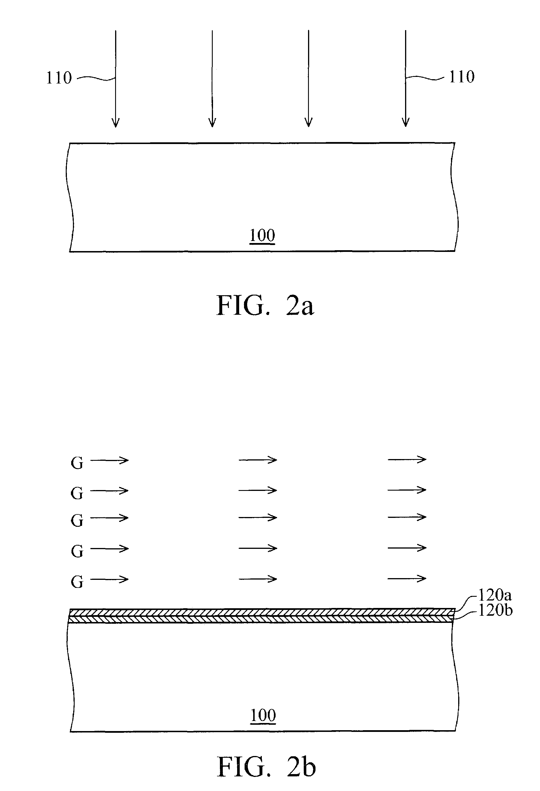
[0027]In FIG. 2a, a semiconductor substrate 100, for example a silicon substrate, having an exposed silicon surface (a surface of the substrate 100) thereon is provided. Next, an ion implant process 110 is performed to implant nitrogen atoms with a predetermined dosage between 1*1014 atoms / cm2 and 5*1017 atoms / cm2 into the substrate 100. A gas source of the nitrogen atoms for the ion implant process 110 can be nitrogen gas (N2).
[0028]In FIG. 2b, a thermal nitridation process (not shown), for example a furnace nitridation process of a rapid thermal nitridation (RTN) process, is performed. Heaters (not shown) disposed in a reactor heat the substrate 100 to a predetermined process temperature between 500° C. and 1200° C. Then a nitrogen-containing gas G is provided and thermally decomposed under the process temperature to liberate nitrogen ato...
PUM
| Property | Measurement | Unit |
|---|---|---|
| Temperature | aaaaa | aaaaa |
| Temperature | aaaaa | aaaaa |
| Energy | aaaaa | aaaaa |
Abstract
Description
Claims
Application Information