Inductive device including bond wires

a technology of inductive devices and bond wires, applied in the direction of transformers/react mounting/support/suspension, magnets, magnetic bodies, etc., can solve the problem that separately manufactured inductive devices may introduce unwanted electrical parasitics

Active Publication Date: 2006-02-14
NXP USA INC
View PDF31 Cites 132 Cited by
  • Summary
  • Abstract
  • Description
  • Claims
  • Application Information

AI Technical Summary

Problems solved by technology

Furthermore, separately manufactured inductive devices may introduce unwanted electrical parasitics due to the connectors of the pre-assembled part.

Method used


Image

  • Inductive device including bond wires
  • Inductive device including bond wires
  • Inductive device including bond wires

Examples


Embodiment Construction

[0015]The following sets forth a detailed description of a mode for carrying out the invention. The description is intended to be illustrative of the invention and should not be taken to be limiting.

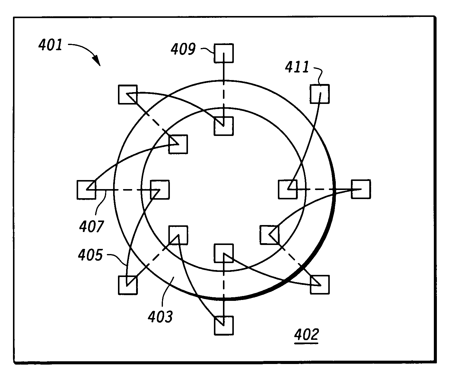
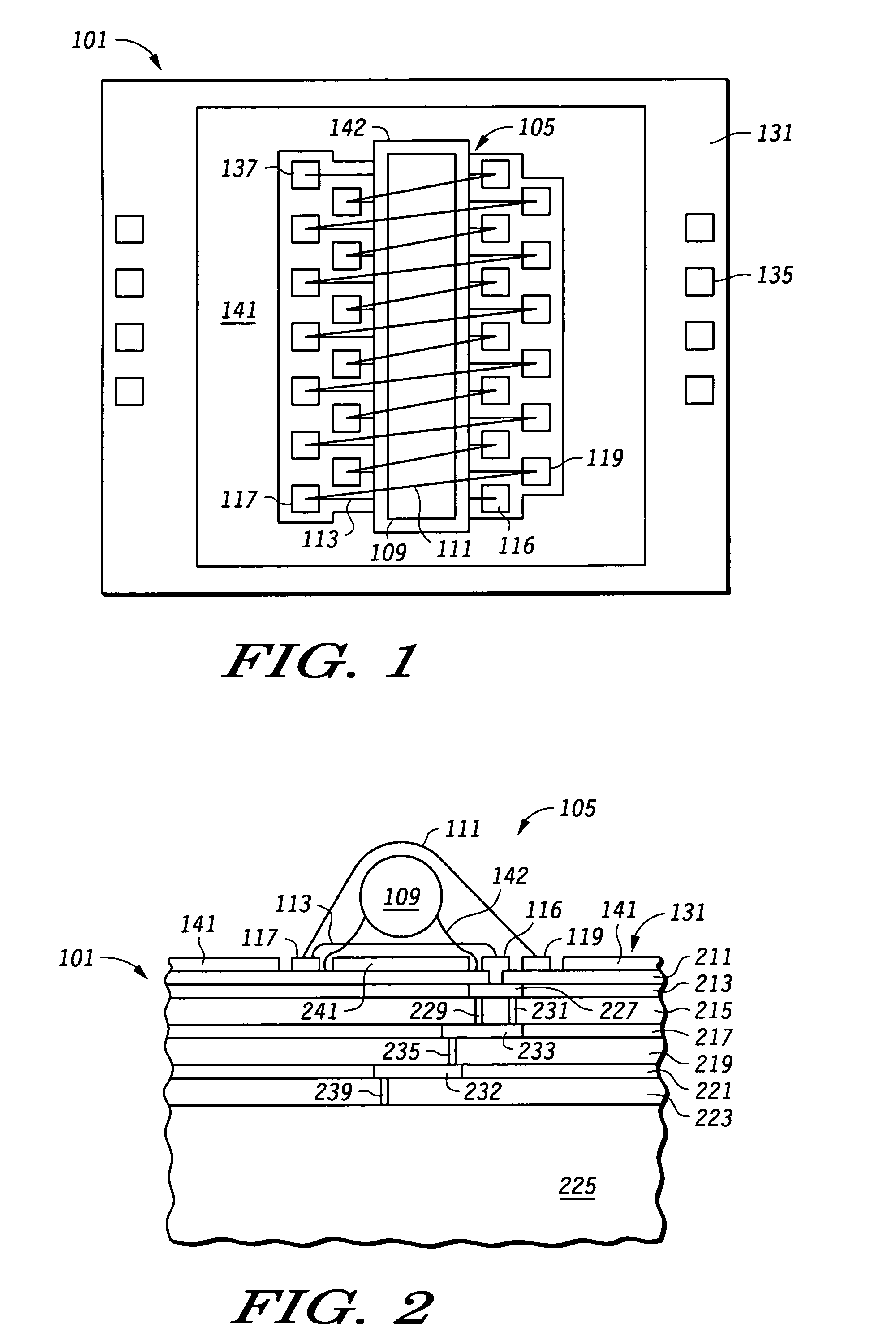
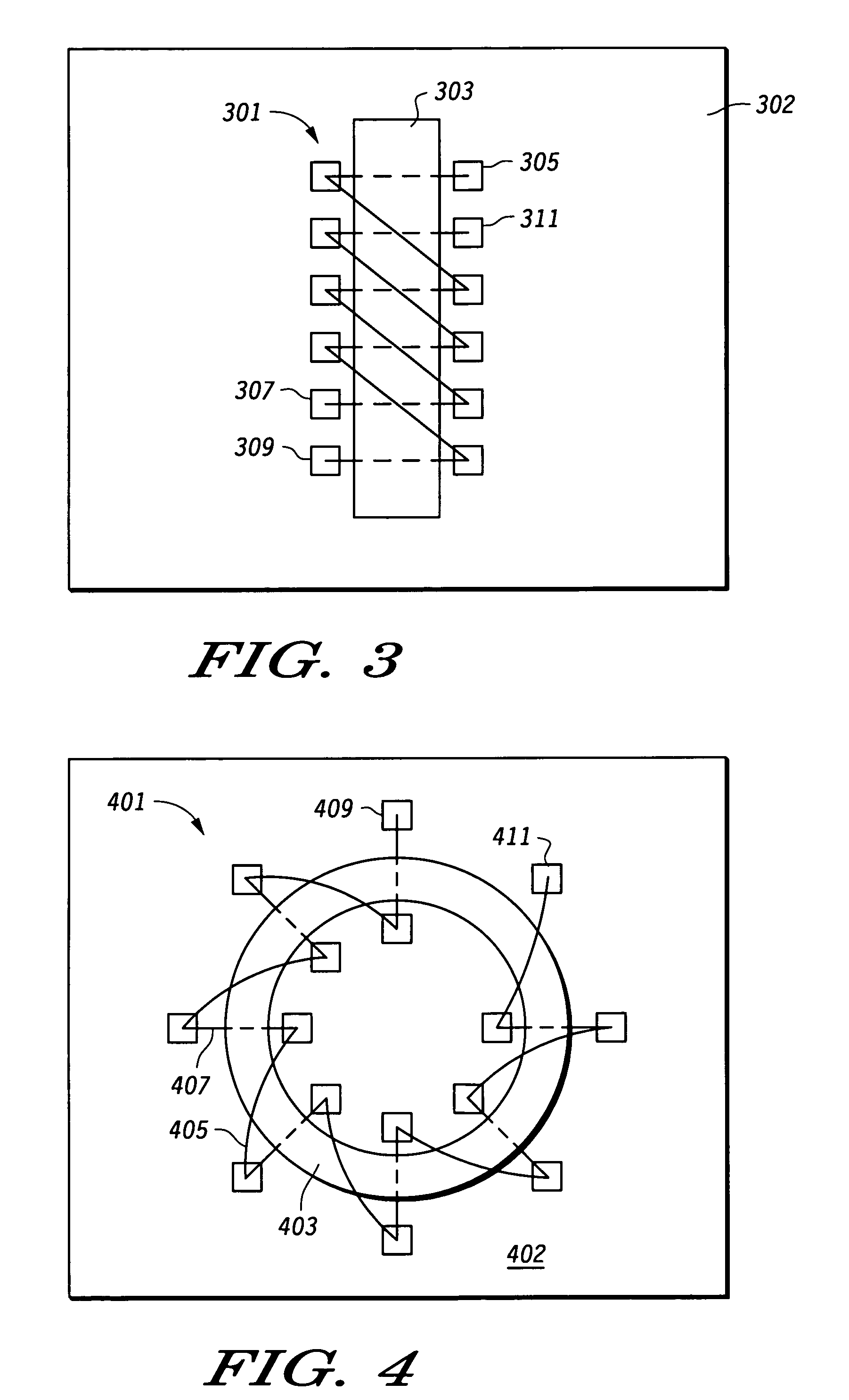
[0016]FIG. 1 is a top view of a integrated circuit die according to the present invention. An inductor 105 is located on a top side 131 of die 101. Inductor 105 includes a first set of bond wires (e.g. 113) including a portion located between a core 109 of magnetic material and the top side 131 of die 101 and a second set of bonding wires e.g. 111 including a portion located over core 109. In one embodiment core 109 is made of a ferrite material, but may include other types of magnetic material in other embodiments, e.g. ferromagnetic material. Each of the bond wires of the first and second sets are bonded to a pair of bond pads (e.g. 117 and 119 for bond wire 111) and function as segments of a coil around core 109 of inductor 105. Bond wires 111 and 113 are made of a conductive material...


PUM

PropertyMeasurementUnit
magneticaaaaaaaaaa
shapeaaaaaaaaaa
semiconductoraaaaaaaaaa

Abstract

An inductive device (105) is formed above a substrate (225) having a conductive coil formed around a core (109). The coil comprises segments formed from a first plurality of bond wires (113) and a second plurality of bond wires (111). The first plurality of bond wires (113) extends between the core (109) and the substrate (225). Each of the first plurality of bond wires is coupled to two of a plurality of wire bond pads (117, 116). The second plurality of bond wires (111) extends over the core (109) and is coupled between two of the plurality of wire bond pads (117, 119). A shield (141) includes a portion that is positioned between the core (109) and the substrate (225).

Description

BACKGROUND OF THE INVENTION[0001]1. Field of the Invention[0002]This invention relates in general to electronic circuits and in particular to inductive devices for electronic circuits.[0003]2. Description of the Related Art[0004]Inductor devices are utilized in electronic devices including e.g. radio frequency electronic devices. Examples of inductive devices include transformers and inductors. In some packaged electronic devices, inductive devices are manufactured separately and then added during the assembly of the packaged electronic device. With other systems, an inductive device may be formed with copper traces on a die.[0005]Utilizing pre-assembled inductive devices in an electronic device may require additional assembly processes for the manufacture of the electronic device. Furthermore, separately manufactured inductive devices may introduce unwanted electrical parasitics due to the connectors of the pre-assembled part.[0006]What is needed is an improved inductive device for...

Claims


Application Information

Patent Timeline
Patent Type & Authority Patents(United States)
IPC IPC(8): H01F27/06H01F5/00H01F17/00H01F41/04H01L23/522
CPCH01F17/0033H01F41/046H01L23/5227H01L23/645H01L2224/4813H01L2924/01079Y10T29/4902H01L2924/14H01L2924/30107H01L2924/3025H01L24/48H01L2924/09701H01L24/45H01L2224/45124H01L2224/45144H01L2224/45147H01L2924/00014H01L2224/45015H01L2924/207
Inventor ZHOU, YAPINGDOWNEY, SUSAN H.CHOPIN, SHEILA F.TRAN, TU-ANHWOOSLEY, ALAN H.HARPER, PETER R.PELLEY, III, PERRY H.
Owner NXP USA INC
Why Eureka
Try Eureka