

Transconductance device employing native MOS transistors
a technology of mos transistors and transistors, applied in the field of electrical systems, can solve the problems of adverse effects of source-bulk voltage (vsb) on mos transistors, limited dynamic range of control voltage in gyrators, adverse effects of transconductance, etc., and achieve the effect of improving the response to noise in semiconductor chips
- Summary
- Abstract
- Description
- Claims
- Application Information
AI Technical Summary
Benefits of technology
Problems solved by technology
Method used
Image

Examples
Embodiment Construction
[0022]FIG. 5 is a functional block diagram of a ring oscillator which generates a control voltage, Vc, for controlling low pass filters 24, 25 in FIG. 1. The ring oscillator includes a voltage controlled oscillator 42 in a phase lock loop including a phase / frequency detector 44 which receives the output of Vco 42 and compares the output with a reference frequency from crystal oscillator 46. The phase and frequency difference detected by detector 44 is applied to a charge pump 48 which generates a voltage for controlling Vco 42. The voltage from charge pump 48 is the control voltage, Vc, which is also applied to control transconductance devices in low pass filters 24, 25.
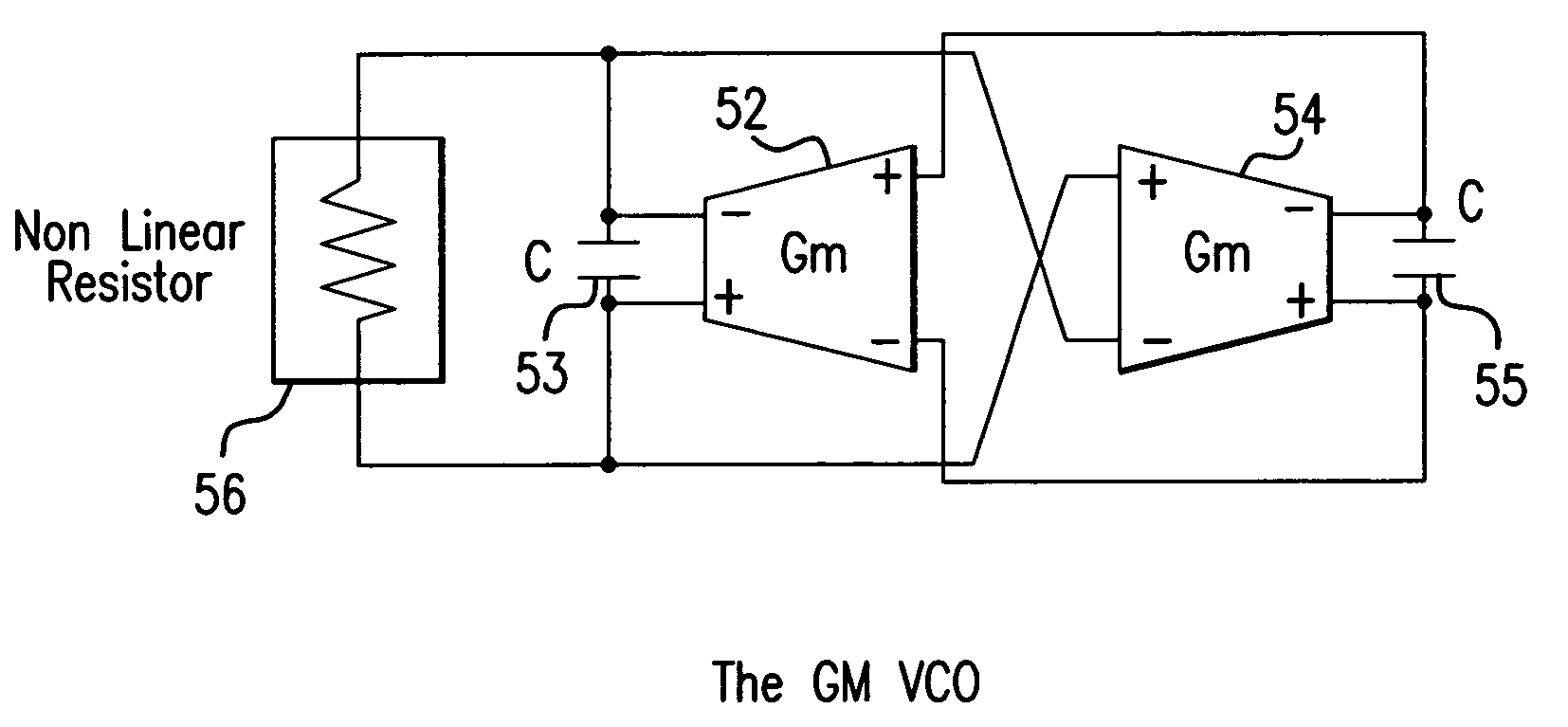
[0023]FIG. 6 is a schematic of Vco 42 implemented as a second order harmonic oscillator including cross coupled transconductance cells 52, 54, and capacitors 53, 55 and a non-linear resistor 56. As noted above, the control voltage generated by ring oscillator of FIG. 5 is used to control the transconductance, GM, sta...
PUM
 Abstract
Description
Claims
Application Information