Transconductor circuit for compensating the distortion of output current

a technology of output current and transistor, applied in the field of transistor circuit, can solve the problems of deteriorating integration density and operation speed, increasing the size of semiconductor chips,

Inactive Publication Date: 2006-05-02
ELECTRONICS & TELECOMM RES INST
View PDF8 Cites 9 Cited by
  • Summary
  • Abstract
  • Description
  • Claims
  • Application Information

AI Technical Summary

Problems solved by technology

However, the increase in the magnitude of the resistor R1 results in increasing the size of semiconductor chips and parasitic capacitance, which deteriorates integration density and operation speed.

Method used


Image

  • Transconductor circuit for compensating the distortion of output current
  • Transconductor circuit for compensating the distortion of output current
  • Transconductor circuit for compensating the distortion of output current

Examples


Embodiment Construction

[0031]The present invention will now be described more fully with reference to the accompanying drawings, in which exemplary embodiments of the invention are shown. The invention may, however, be embodied in many different forms and should not be construed as being limited to the embodiments set forth herein; rather, these embodiments are provided so that this disclosure will be thorough and complete, and will fully convey the concept of the invention to those skilled in the art. In the drawings, the thicknesses of layers and regions are exaggerated for clarity. Like reference numerals in the drawings denote like elements, and thus their description will be omitted.

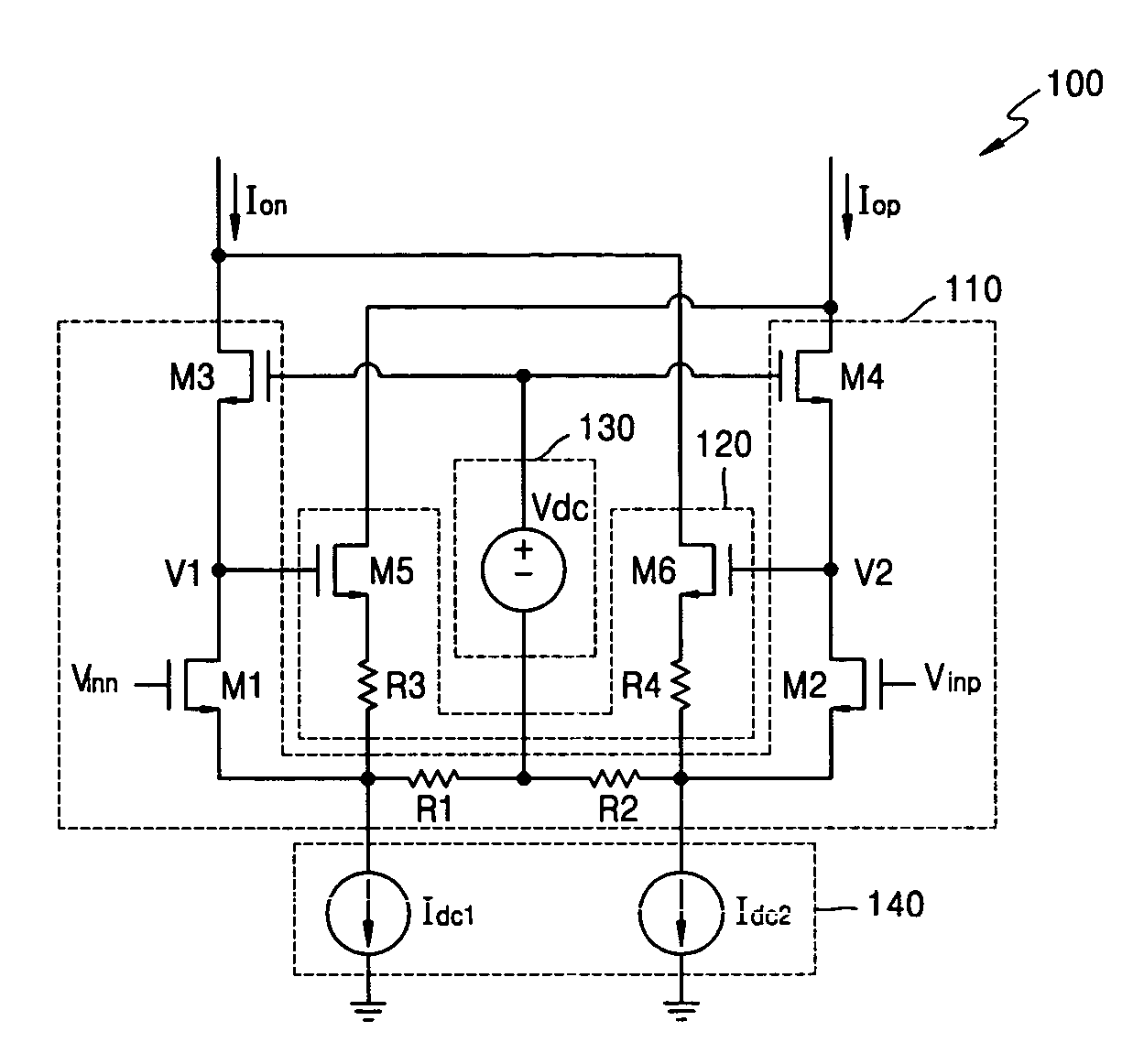
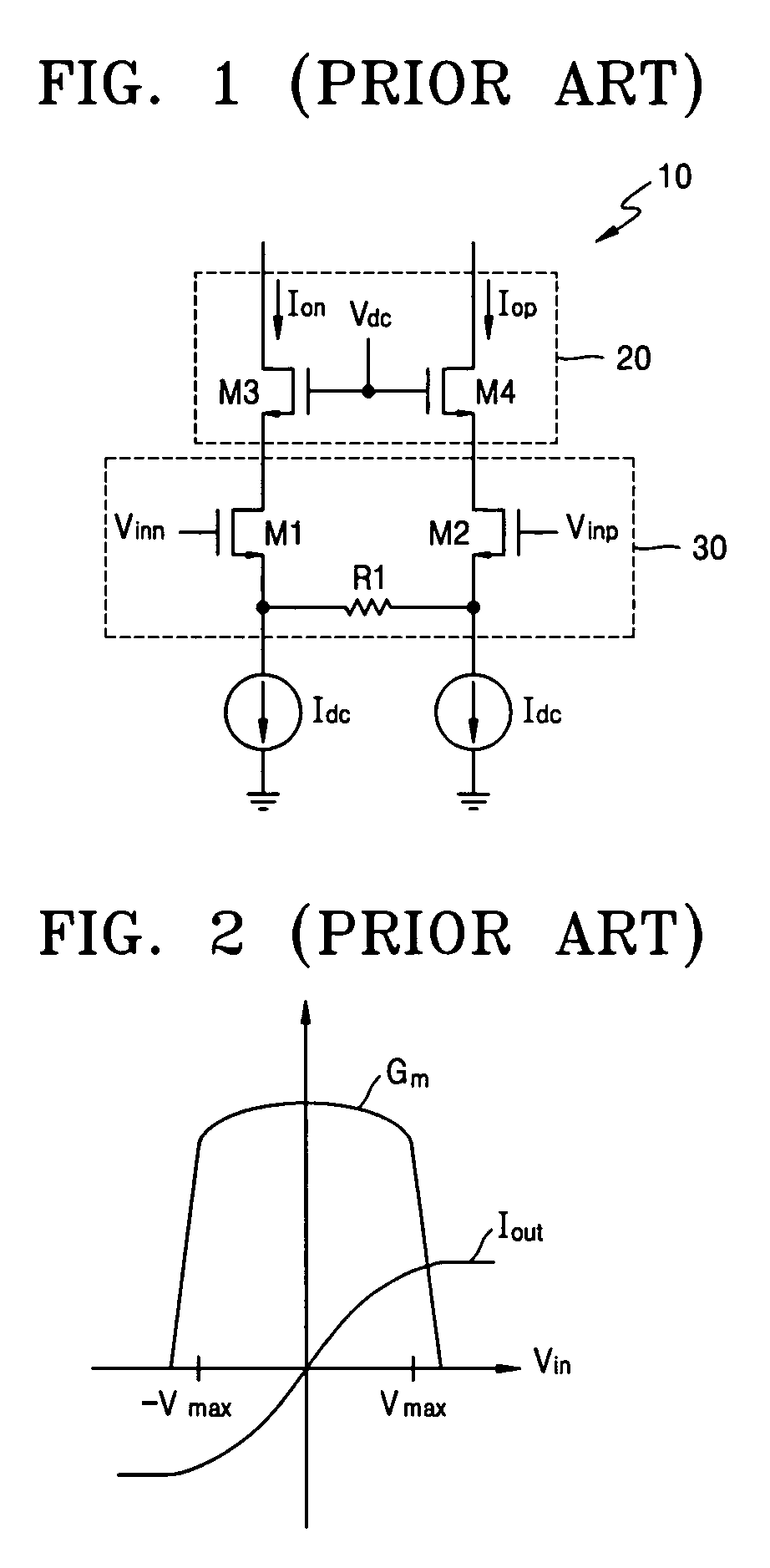
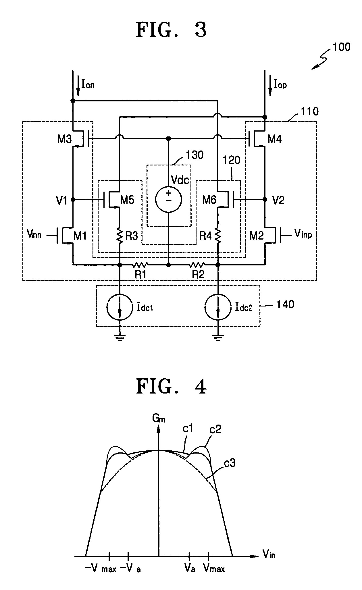
[0032]FIG. 3 is a circuit diagram of a transconductor circuit, according to an embodiment of the present invention. Referring to FIG. 3, a transconductor circuit 100 includes a main circuitry 110, an auxiliary circuitry 120, a variable voltage supply 130, and a current source 140.

[0033]The main circuitry 110 is a differen...


PUM


Abstract

Provided is a transconductor circuit for compensating distortion of an output current without reducing the size of chips and operation speed characteristics. The transconductor circuit includes a main circuitry which is a differential pair with source degeneration and to which a predetermined input voltage is applied, an auxiliary circuitry which is connected to nodes of the main circuitry to compensate the distortion of the output current, a variable voltage supply which controls a depth or degree of a distortion compensation operation for the output current, and a current source which supplies the main circuitry with constant bias.

Description

BACKGROUND OF THE INVENTION[0001]This application claims the priority of Korean Patent Application No. 2003-95399, filed on Dec. 23, 2003, in the Korean Intellectual Property Office, the disclosure of which is incorporated herein in its entirety by reference.[0002]1. Field of the Invention[0003]The present invention relates to a transconductor circuit, and more particularly, to a transconductor circuit including metal oxide semiconductor (MOS) transistors so as to prevent an output current from being distorted.[0004]2. Description of the Related Art[0005]In general, transconductors are circuits that convert a voltage into a current to process an electric signal. In other words, when a predetermined voltage is applied to the transconductors, the transconductors output a current value. Such a transconductor is generally used in an analog signal processor such as a filter, a gain variable amplifier, or the like.[0006]The transconductor is processed by a highly integrated analog signal ...

Claims


Application Information

Patent Timeline
Patent Type & Authority Patents(United States)
IPC IPC(8): H03K3/00H03D1/00H03D7/14H03F1/32H03F3/45
CPCH03D7/1441H03F1/3211H03D7/1458H03D7/1491H03F3/45197H03D2200/0043H03F3/45
Inventor LEE, BEAUNG WOOPARK, MUN YANG
Owner ELECTRONICS & TELECOMM RES INST
Why Eureka
Try Eureka