
Light emitting device and method of driving the same

a technology of light emitting devices and driving transistors, applied in static indicating devices, instruments, animations, etc., can solve problems such as weakening the resistance of driving transistors to fluctuation in characteristic characteristics

Inactive Publication Date: 2006-08-08
SEMICON ENERGY LAB CO LTD
View PDF28 Cites 189 Cited by
  • Summary
  • Abstract
  • Description
  • Claims
  • Application Information

AI Technical Summary

Benefits of technology

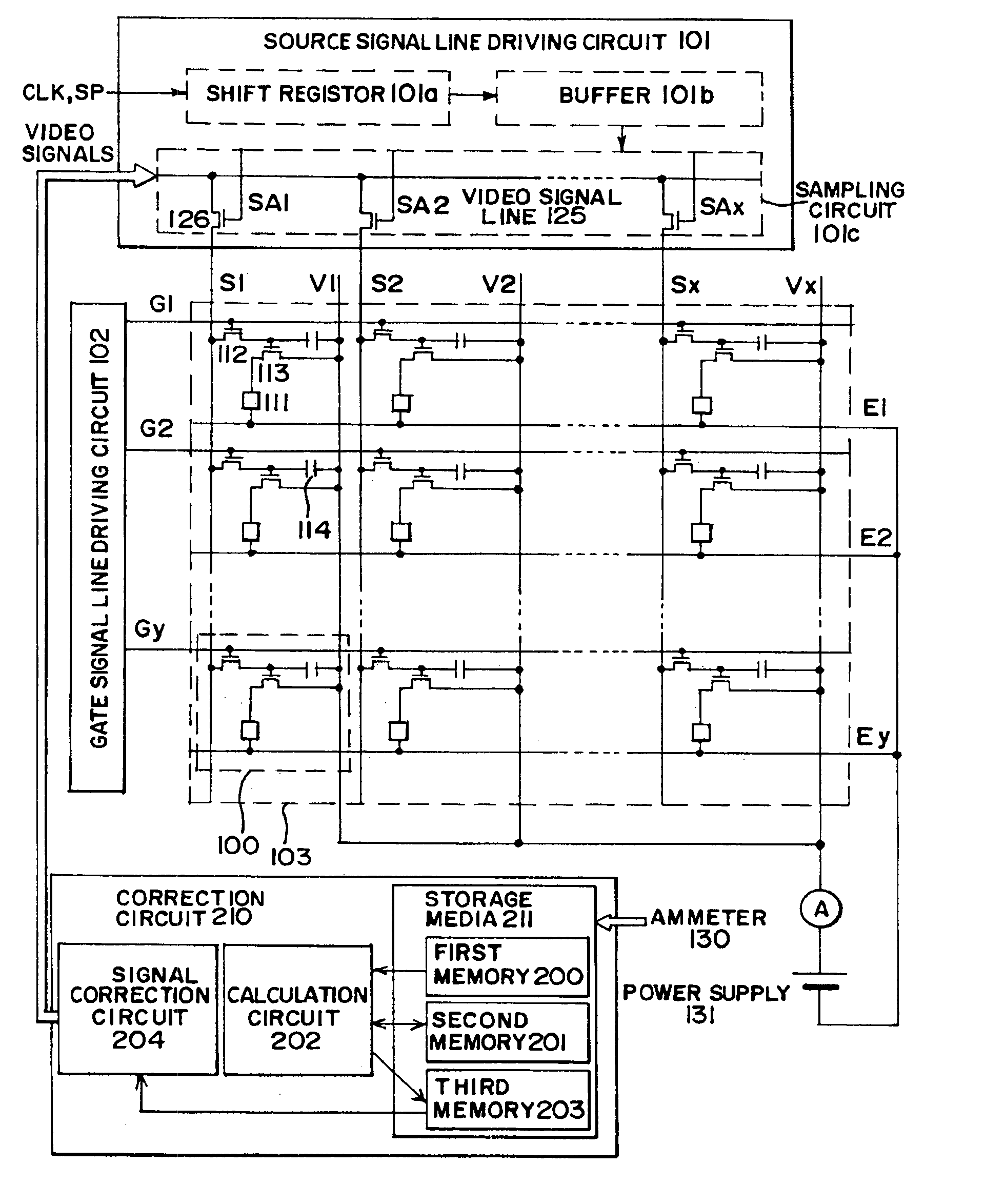
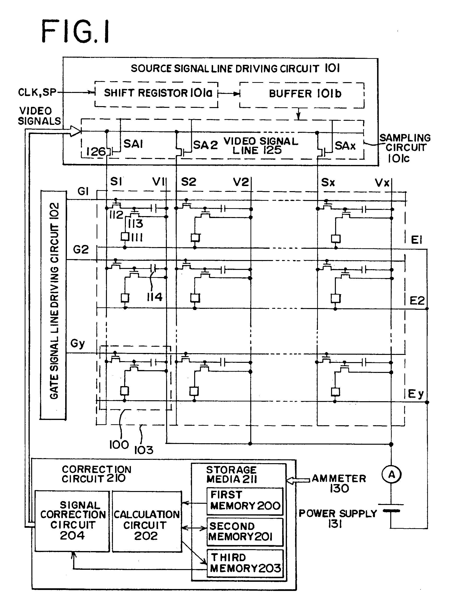
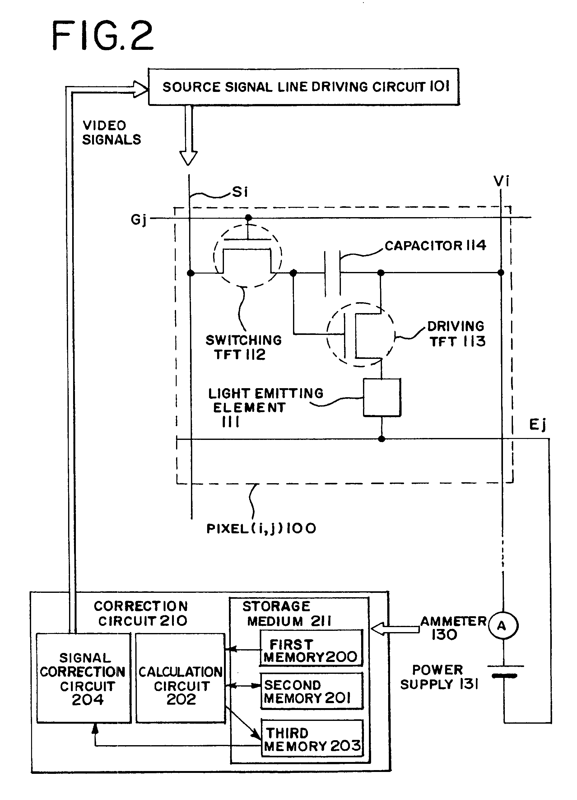
The present invention provides a light emitting device and its driving method that can remove the influence of fluctuation in characteristic among driving transistors and obtain a clear multi-gray scale display. The device includes current measuring means for measuring the current value of pixels, calculating means for calculating interpolation functions corresponding to the pixels, and memory means for storing interpolation functions for each pixel. The device can correct video signals using the interpolation functions to obtain the desired luminance for each pixel. The technical effects of the invention include reducing the impact of fluctuation in characteristic among driving transistors and improving the display quality of light emitting devices.

Problems solved by technology

However, the analog method described above has such a drawback that it is very weak against fluctuation in characteristic among driving transistors.
Analog driving methods are thus responsive to fluctuation in characteristic among driving transistors and it has been a liability in gray scale display by conventional active light emitting devices.

Method used


Image

  • Light emitting device and method of driving the same
  • Light emitting device and method of driving the same
  • Light emitting device and method of driving the same

Examples


embodiment 1

[0135]The present invention is also applicable to a light emitting device with a pixel having a structure different from the one in FIG. 2. This embodiment describes an example thereof with reference to FIG. 6 and FIGS. 18B and 18C.

[0136]A pixel (i, j) shown in FIG. 6 has a light emitting element 311, a switching transistor 312, a driving transistor 313, an erasing transistor 315, and a capacitor storage 314. The pixel (i, j) is placed in a region surrounded by a source signal line (Si), a power supply line (Vi), a gate signal line (Gj), and an erasing gate signal line (Rj).

[0137]A gate electrode of the switching transistor 312 is connected to a gate signal line (Gj). The switching transistor 312 has a source region and a drain region one of which is connected to a source signal line (Si) and the other of which is connected to a gate electrode of the driving transistor 313. The switching transistor 312 is a transistor functioning as a switching element when a signal is inputted to t...

embodiment 2

[0153]This embodiment describes an example of sectional structure of a pixel with reference to FIG. 7.

[0154]In FIG. 7, a switching transistor 4502, which is an n-channel transistor formed by a known method, is provided on a substrate 4501. The transistor in this embodiment has a double gate structure. However, a single gate structure, a triple gate structure, or a multi-gate structure having more than three gates may be employed instead. The switching transistor 4502 may be a p-channel transistor formed by a known method.

[0155]A driving transistor 4503 is an n-channel transistor formed by a known method. A drain wire 4504 of the switching transistor 4502 is electrically connected to a gate electrode 4506 of the driving transistor 4503 through a wire (not shown in the drawing).

[0156]The driving transistor 4503 is an element for controlling the amount of current flowing in a light emitting element 4510, and a large amount of current flows through the driving transistor to raise the ri...

embodiment 3

[0180]In this embodiment, an appearance view of the light emitting device is described with reference to FIGS. 8A to 8B.

[0181]FIG. 8A is a top view of the light emitting device, FIG. 8B is a cross sectional view taken along with a line A-A′ of FIG. 8A, and FIG. 8C is a cross sectional view taken along with a line B-B′ of FIG. 8A.

[0182]A seal member 4009 is provided so as to surround a pixel portion 4002, a source signal line driving circuit 4003, and the first and the second gate signal line driving circuits 4004a, 4004b, which are provided on a substrate 4001. Further, a sealing material 4008 is provided on the pixel section 4002, the source signal line driving circuit 4003, and the first and the second gate signal line driving circuits 4004a, 4004b. The pixel section 4002, the source signal line driving circuit 4003, and the first and the second gate signal line driving circuits 4004a, 4004b are sealed by the substrate 4001, the seal member 4009 and the sealing material 4008 toget...


PUM


Abstract

The present invention specifies the characteristic of a driving transistor provided in a pixel and corrects a video signal to be inputted to the pixel based on the specification. As a result, a light emitting device and its driving method in which influence of fluctuation in characteristic among transistors is removed to obtain clear multi-gray scale are provided. The present invention can also provide a light emitting device and its driving method in which a change with age in amount of current flowing between two electrodes of a light emitting element is reduced to obtain clear multi-gray scale display.

Description

BACKGROUND OF THE INVENTION[0001]1. Field of the Invention[0002]The present invention relates to a light emitting device in which a light emitting element and a transistor for controlling the light emitting element are provided on a semiconductor substrate or an insulating surface, and to a method of driving the light emitting device. More specifically, the invention relates to a light emitting device and method of driving the same in which influence of fluctuation in characteristic of transistors which control light emitting elements is removed. The present invention belongs to a technical field related to a light emitting device using a semiconductor element such as a transistor.[0003]2. Description of the Related Art[0004]In recent years, development of light emitting devices using light emitting elements (image display devices) is being advanced. Light emitting devices are roughly divided into passive type and active type. Active light emitting devices each have a light emitting...

Claims


Application Information

Patent Timeline
Patent Type & Authority Patents(United States)
IPC IPC(8): G09G3/10G06T13/00G09G3/00G09G3/20G09G3/30G09G3/32H01L51/50
CPCG09G3/3233G09G2300/0842G09G2310/0251G09G2320/02G09G3/3291G09G2320/0285G09G2320/029G09G2320/0295G09G2320/043G09G2320/0257H10K59/10G09G3/2059G09G3/22G09G2340/14
Inventor KIMURA, HAJIME
Owner SEMICON ENERGY LAB CO LTD
Learn More