

Setting black levels in organic EL display devices
a technology of electroluminescent devices and black levels, which is applied in the direction of electroluminescent light sources, static indicating devices, instruments, etc., can solve the problems of accelerating the deterioration of oled elements, unable to compensate for the change of black and/or white levels, and/or display luminance may be reduced, and/or image luminance may increase.
- Summary
- Abstract
- Description
- Claims
- Application Information
AI Technical Summary
Benefits of technology
Problems solved by technology
Method used
Image

Examples
Embodiment Construction
[0026]In the following, preferred embodiments of the present invention will be described with reference to the following drawings.
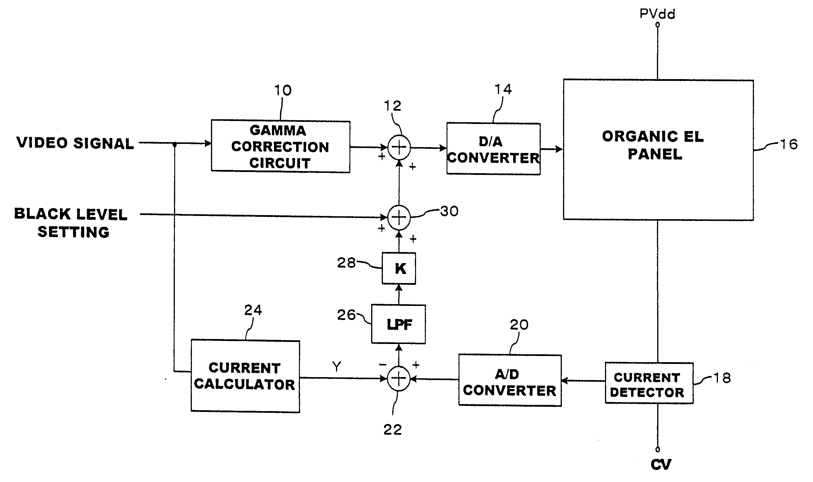
[0027]FIG. 3 shows a structure of a device of a preferred embodiment of the present invention. In this device, a video signal including image data for each pixel is input to a gamma correction circuit 10 for correcting a video signal according to predetermined gamma propriety so that the resultant image data has linear relationship with an amount of a current flowing in a pixel. A video signal subjected to gamma correction is supplied to an adder 12 for addition of a black level setting level, so that an output of the adder 12 resultantly constitutes data concerning a driving current for each pixel.
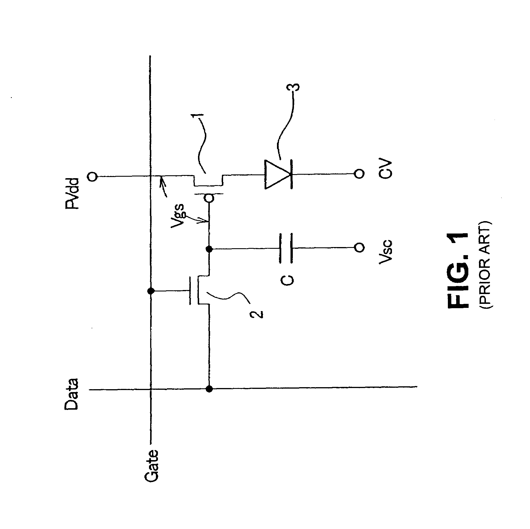
[0028]The output of the adder 12 is supplied to a D / A converter 14 for conversion into an analog signal, which is supplied to an organic EL panel 16, which includes pixel circuits, as shown in FIG. 1, arranged in a matrix.
[0029]Note that a signal from the D / A c...
PUM
 Abstract
Description
Claims
Application Information