Expansible interface for modularized printed circuit boards

a printed circuit board and modularization technology, applied in the direction of printed circuit structure associations, printed circuit aspects, coupling device connections, etc., can solve the problems of reducing the space occupied by the pcb, the above-mentioned modularized pcbs are inevitably large, and the electronic device employing the above-mentioned modularized pcbs is not adapted to the market requirements

Inactive Publication Date: 2007-01-30
HON HAI PRECISION IND CO LTD
View PDF8 Cites 43 Cited by
  • Summary
  • Abstract
  • Description
  • Claims
  • Application Information

AI Technical Summary

Problems solved by technology

However, the electronic device employing the above-mentioned modularized PCBs is not adapted to the market requirements.
Because the electronic devices are developed toward light, thin, short and small, the above-mentioned modularized PCBs are inevitably large.
Although the space occupied by the PCBs is reduced, the communication between the primary PCB and the subsidiary PCB is still inconvenient to use.

Method used


Image

  • Expansible interface for modularized printed circuit boards
  • Expansible interface for modularized printed circuit boards
  • Expansible interface for modularized printed circuit boards

Examples


Embodiment Construction

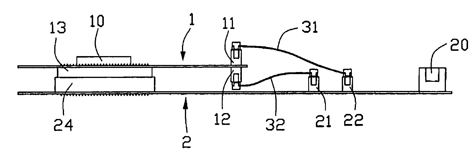
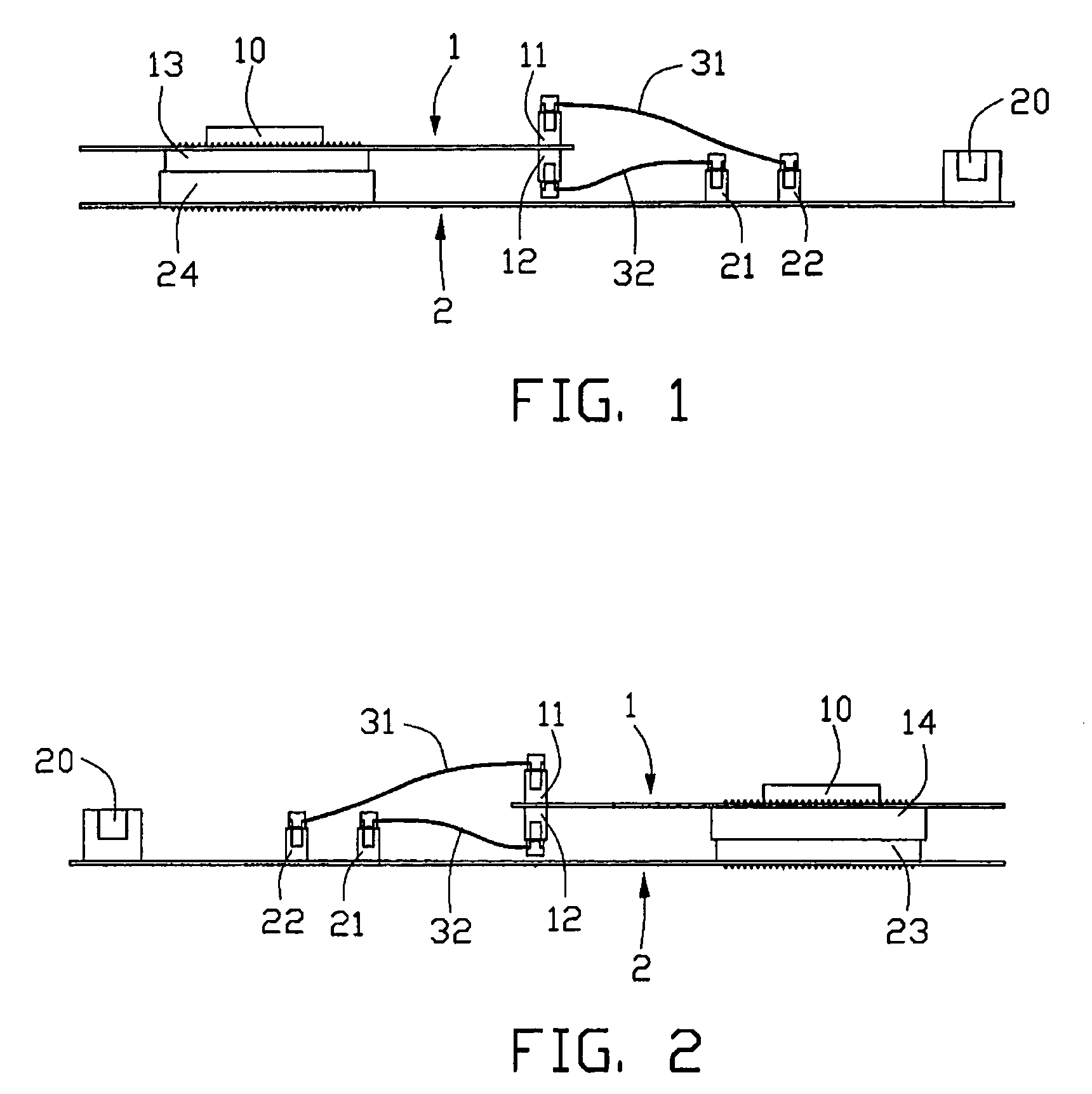
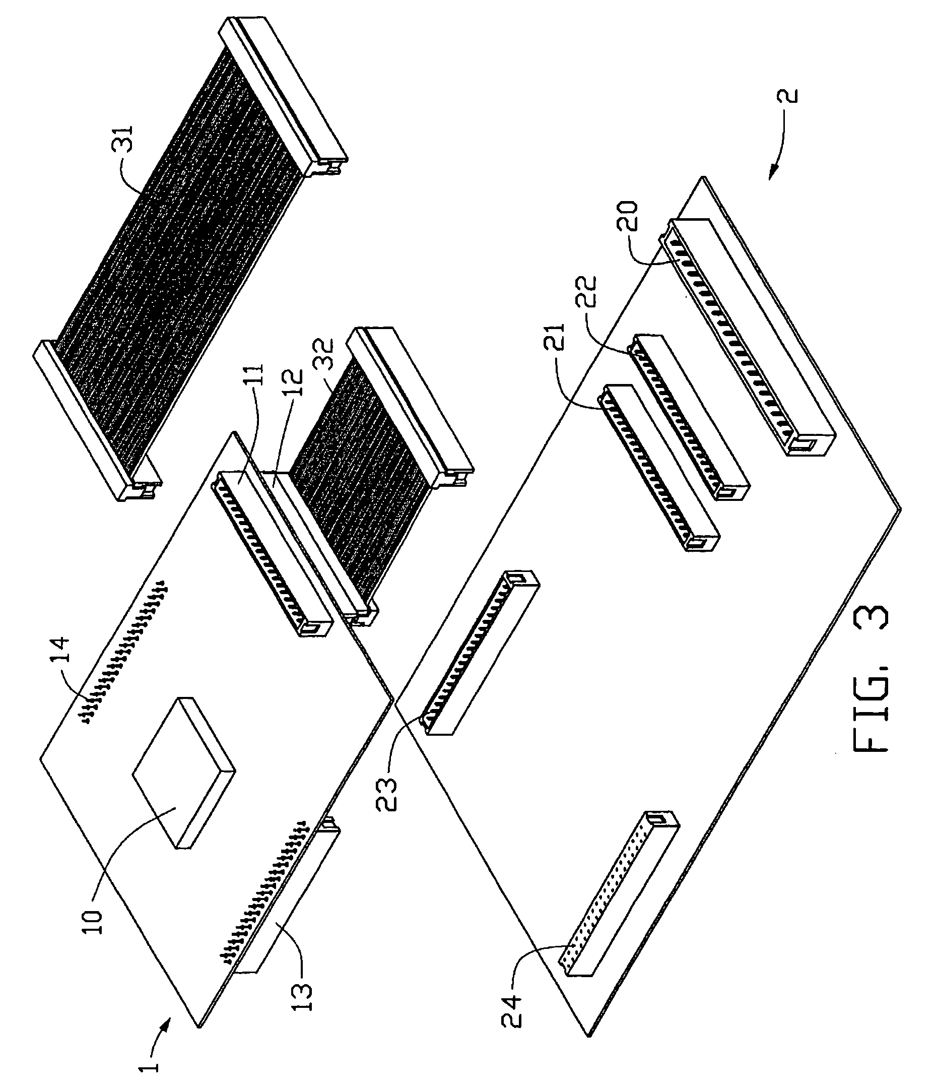
[0015]FIG. 1 is a side plan view of an expansible interface for modularized PCBs in accordance with the preferred embodiment of the present invention. FIG. 2 is an opposite side plan view of the expansible interface for modularized PCBs in accordance with the preferred embodiment of the present invention. FIG. 3 is an exploded, isometric view of the expansible interface for modularized PCBs in accordance with the preferred embodiment of the present invention. In the preferred embodiment, the modularized PCBs comprise a primary PCB 1, a subsidiary PCB 2, and connectors 13, 14, 23, 24. The connectors 13, 14 are fixed on a same side of the primary PCB 1, and the connectors 23, 24 are fixed on a same side of the subsidiary PCB 2. In addition, the primary PCB 1 is assembled with connectors 11, 12 respectively on an upper side and on a lower side thereof, and a CPU 10 on the upper side thereof. The subsidiary PCB 2 is assembled with connectors 21, 22 and a plurality of PCI slots 20 (only ...


PUM


Abstract

An expansible interface for expanding different kinds of data from a primary printed circuit board (PCB) (1) to a subsidiary PCB (2), the primary PCB is fixed with board-to-board connectors (13, 14) and flexible printed circuit (FPC) connectors (11, 12), and the subsidiary PCB is fixed with the corresponding board-to-board connectors (23, 24) and the corresponding FPC connectors (21, 22). The board-to-board connectors are directly electrically connected with each other for transmitting a data that is not a Peripheral Component Interconnect (PCI) data from the primary PCB to the subsidiary PCB; the FPC connectors are electrically connected with each other via cables (31, 32) for transmitting the PCI data from the primary PCB to the subsidiary PCB.

Description

BACKGROUND OF THE INVENTION[0001]1. Field of the Invention[0002]The present invention relates to expansible interfaces of electronic devices, and particularly to an expansible interface for modularized printed circuit boards (PCBs).[0003]2. Prior Art[0004]Nowadays, modularized PCBs that comprise a primary PCB and a subsidiary PCB are broadly employed in many electronic devices. The primary PCB of the modularized PCBs is assembled with a plurality of main components such as a central processing unit (CPU) and a memory. The subsidiary PCB of the modularized PCBs is an expansible board ancillary to the primary PCB, and is coupled to the primary PCB to form a unified PCB assembly. The modularized PCBs are generally used in routers, uninterruptible power supplies (UPSs), and so on.[0005]Taiwan Patent Publication No. 458,306, issued on Oct. 01, 2001, discloses an expansible interface for modularized PCBs. Referring to FIG. 4, a primary PCB 5 is provided with a CPU 51 and a connector 50. A...

Claims


Application Information

Patent Timeline
Patent Type & Authority Patents(United States)
IPC IPC(8): H01R12/00H01R12/14H01R12/24H01R12/71H01R12/79H05K1/00H05K1/14
CPCH01R12/716H05K1/147H01R23/667H05K2201/10189H01R12/725
Inventor HSIEH, MING-CHIH
Owner HON HAI PRECISION IND CO LTD
Why Eureka
Try Eureka