Wideband antenna and communication apparatus having the antenna
a communication apparatus and antenna technology, applied in the structure of resonant antennas, antennas with plural divergent straight elements, radiating elements, etc., can solve the problem of insufficient extension of the transmitting and receiving band in the required frequency band
- Summary
- Abstract
- Description
- Claims
- Application Information
AI Technical Summary
Benefits of technology
Problems solved by technology
Method used
Image
Examples
first embodiment
[0081](First Embodiment)
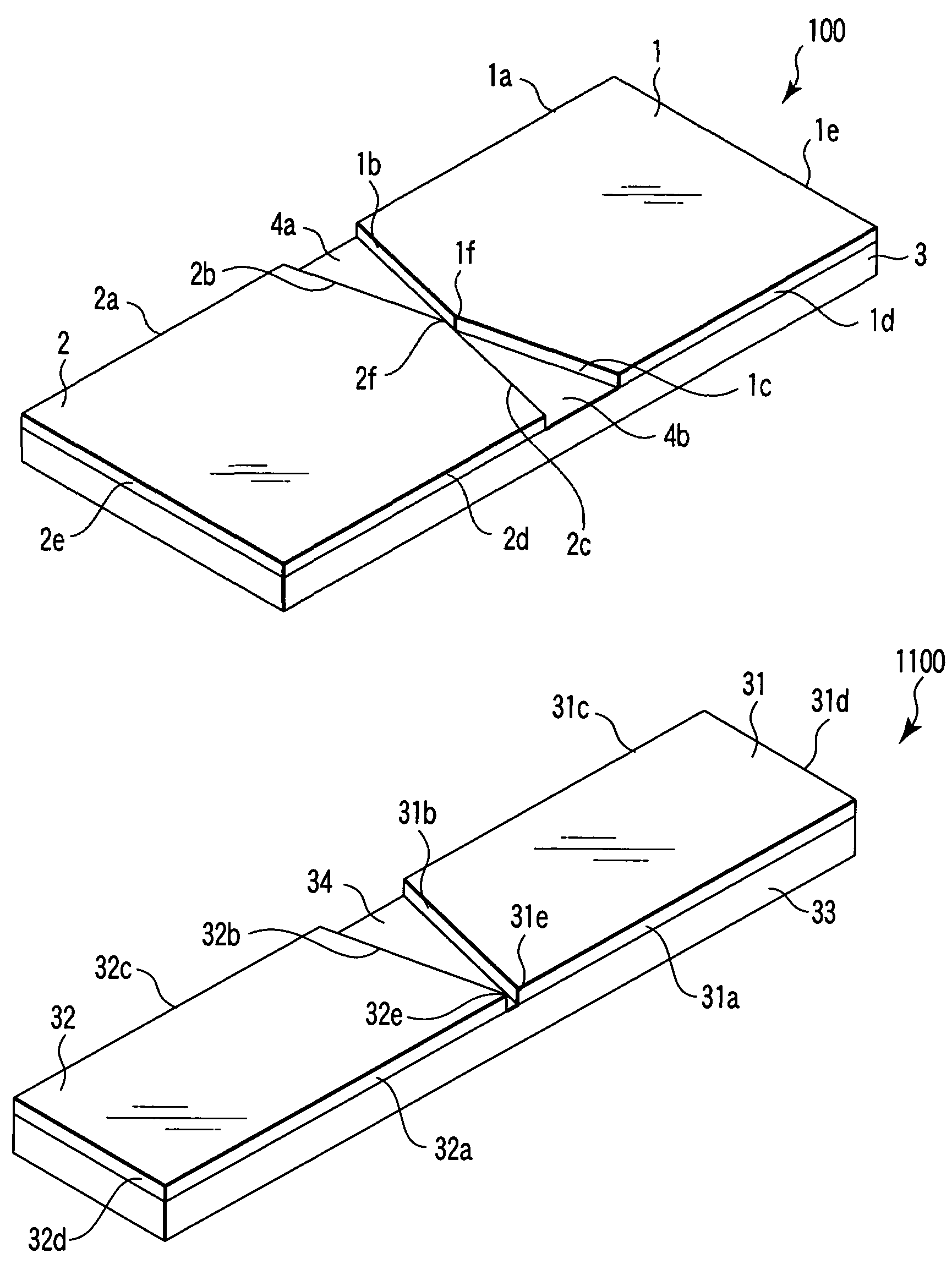
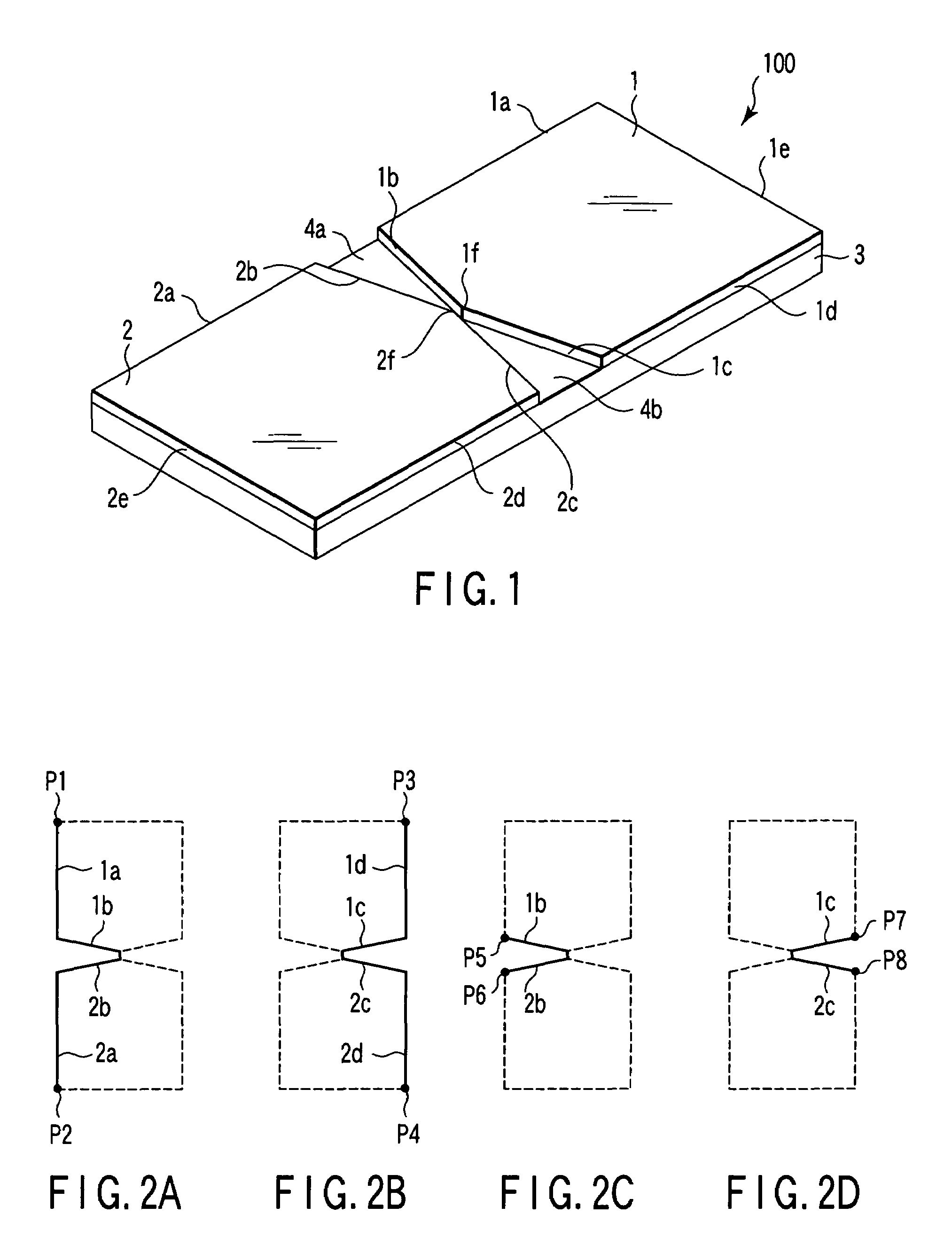
[0082]FIG. 1 is the perspective view showing the structure of the wideband antenna 100 regarding the first embodiment of the invention.
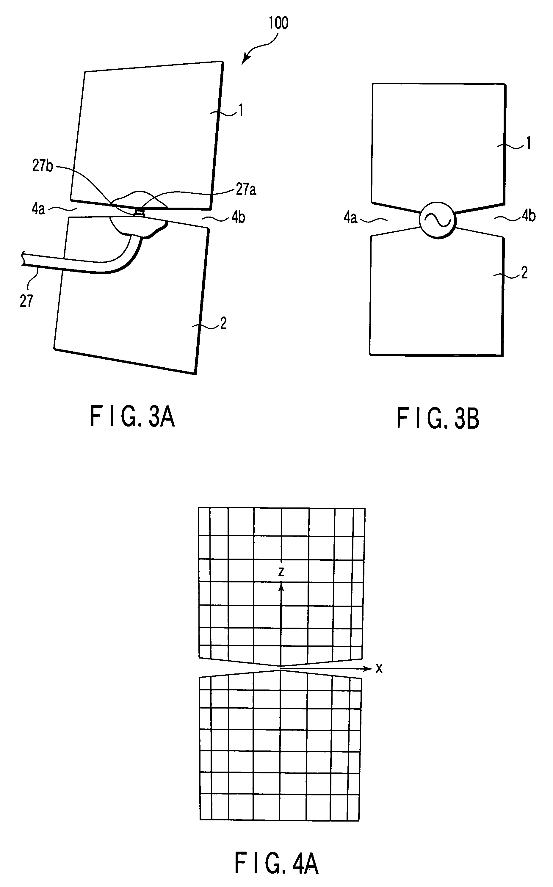
[0083]As shown in FIG. 1, the antenna 100 comprises the conductive elements 1, 2 and a dielectric substrate 3.
[0084]The elements 1, 2 are thin plates made of conductive material. The elements 1, 2 respectively have a pentagonal shape formed so that one side of a rectangular thin plate is linearly notched with the same angle from its center to both sides. The shapes of the elements 1, 2 are approximately congruent with each other.
[0085]Five sides of the element 1 are referred to as sides 1a, 1b, 1c, 1d and 1e as shown FIG. 1. The sides 1b, 1c are inclined sides provided with a shape so as to notch as mentioned above and contact each other. A top 1f is formed at a part at which the sides 1b, 1c contact with each other. The side 1a contacts the side 1b. The side 1d contacts the side 1c. The side 1e contacts the sides 1a, 1d, resp...
second embodiment
[0106](Second Embodiment)
[0107]FIG. 9 is the illustration showing the structure of the wideband antenna 200 regarding the second embodiment of the invention. In FIG. 9, the same parts as those of FIG. 1 designated by the same reference numerals and detailed explanation thereof will be omitted.
[0108]As shown in FIG. 9, the antenna 200 comprises conductive elements 7 and 8. These elements 7, 8 are mounted on a dielectric substrate, but the substrate is not shown.
[0109]The elements 7, 8 are thin plates made of conductive material. The elements 7, 8 respectively have a pentagonal shape formed so that a first side of a rectangular thin plate is linearly notched with the same angle from its center to both sides and so that a second side facing the first side is linearly notched from one end of the second side. The shapes of the elements 7, 8 are approximately congruent with each other.
[0110]Five sides of the element 7 are referred to as sides 7a, 7b, 7c, 7d and 7e as shown in FIG. 9. Five...
third embodiment
[0116](Third Embodiment)
[0117]FIG. 13 is an illustration showing the structure of the wideband antenna 300 regarding the third embodiment of the invention. In FIG. 13 the same parts as that of FIG. 1 designated by the same reference numerals and detailed explanation thereof will be omitted.
[0118]As shown in FIG. 13, the antenna 300 comprises the elements 2 and an element 9. These elements 2, 9 are mounted on a dielectric substrate, but the substrate is not shown in FIG. 13. That is, the antenna 300 is equipped with the element 9 instead of the element 1 of the antenna 100.
[0119]The element 9 is a thin plate made of conductive material. The element 9 has a shape in which a part of the element 1 is notched in rectangle from the side of the side 1e of the element 1 and a notch 9a is provided. The element 9 is arranged opposite to the element 2 in the same positional relationship.
[0120]The element 9 has the sides 1a, 1b, 1c, 1d and the top 1f of the element 1 as they are. These sides ar...
PUM
 Abstract
Description
Claims
Application Information


