Tamper barrier for electronic device

a technology for electronic devices and barriers, applied in the direction of electrical apparatus casings/cabinets/drawers, semiconductor/solid-state device details, instruments, etc., can solve the problems of time-consuming methods and not well suited to automated/mass production

Active Publication Date: 2007-02-20
PITNEY BOWES INC
View PDF55 Cites 98 Cited by
  • Summary
  • Abstract
  • Description
  • Claims
  • Application Information

AI Technical Summary

Problems solved by technology

Due to the manual manipulation required, these methods are typically time consuming and not well suited to automated / mass production.

Method used


Image

  • Tamper barrier for electronic device
  • Tamper barrier for electronic device
  • Tamper barrier for electronic device

Examples


Embodiment Construction

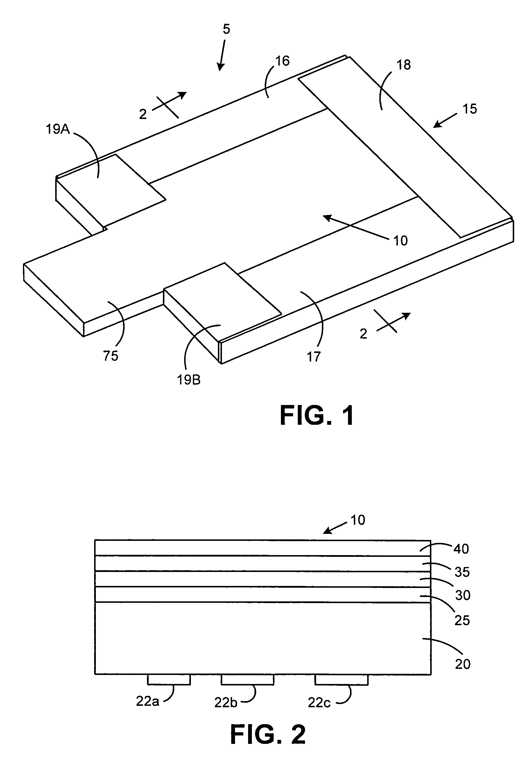
[0016]Referring to FIG. 1, the present invention relates to a PCB assembly, shown at reference numeral 5, that includes a multilayer PCB 10 and a tamper wrap 15 that partially envelops PCB 10. As described in more detail below, PCB 10 is provided with electrical security elements that provide tamper protection in the areas of PCB 10 not covered by tamper wrap 15. Together, these security elements and tamper wrap 15 provide a full envelope of tamper protection for all of the electrical components of PCB 10.

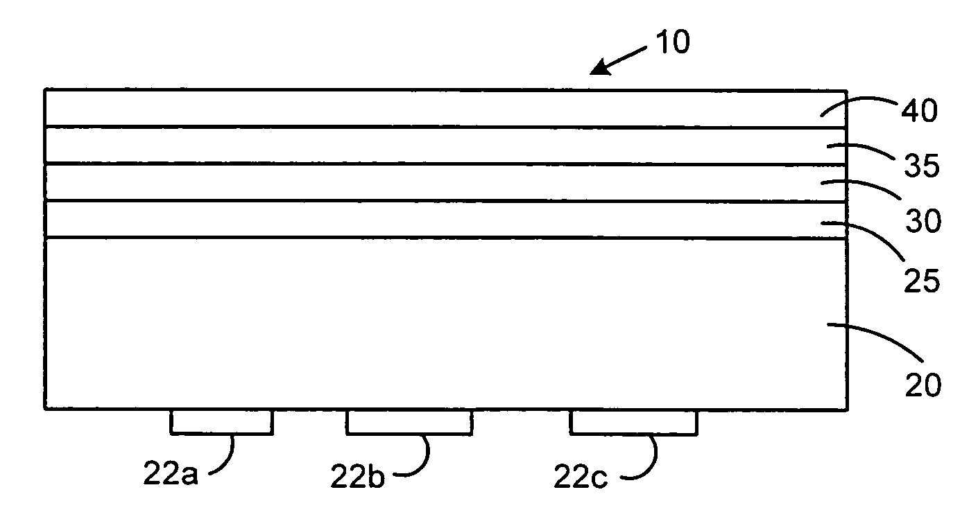
[0017]Referring to FIG. 2, a cross-sectional diagram of PCB 10 taken along lines 2—2 in FIG. 1 is provided which shows each of the layers of PCB 10. Each of the layers of PCB 10 includes a substrate or base, made of, for example, fiberglass or glass epoxy, on which various elements are provided as described herein. PCB circuitry portion 20 actually includes a number of layers, such as those included in a standard PCB, for example, a common six layer PCB. As will be appreciated by t...


PUM

PropertyMeasurementUnit
areaaaaaaaaaaa
flexibleaaaaaaaaaa
electricalaaaaaaaaaa

Abstract

A tamper protected printed circuit board assembly including a printed circuit board and a partially enveloping tamper wrap covering the entirety of the top surface of the printed circuit board and a first portion of the bottom surface of the printed circuit board, wherein a second portion of the bottom surface of the printed circuit board is not covered by the tamper wrap is provided. The printed circuit board includes two security trace layers each having two security traces thereon, preferably in a serpentine pattern. The tamper wrap and the security traces together cover and prevent tampering with the electronic circuitry of the printed circuit board.

Description

CROSS-REFERENCE TO RELATED APPLICATIONS[0001]This application claims the benefit of U.S. Provisional Application Ser. No. 60 / 538,554, filed on Jan. 23, 2004, the specification of which is hereby incorporated by reference.FIELD OF THE INVENTION[0002]The present invention relates to tamper detection and protection for electronic circuitry, and more particularly, to a printed circuit board assembly including a multilayer printed circuit board having a built-in tamper detection element and a partially enveloping tamper detection wrap.BACKGROUND OF THE INVENTION[0003]In many electronic applications, it is often desirable or even required to protect electronic circuitry, such as on a printed circuit board (PCB), from unlawful or unauthorized access. This is especially true for electronic circuitry that includes cryptographic modules or functionality. For example, postage security devices (PSDs) are required by the United States Postal Service to comply with FIPS 140-2 level 3 issued by th...

Claims


Application Information

Patent Timeline
Patent Type & Authority Patents(United States)
IPC IPC(8): H01R12/04H05K5/00G06F21/00H05K1/02
CPCG06F21/87H01L23/576H05K1/0275H05K2201/09263H05K2201/10151Y10T29/49117Y10T29/49144Y10T29/49155Y10T29/4913Y10T29/49128Y10T29/49124H01L2924/0002H01L2924/00
Inventor HEITMANN, KJELL ACLARK, DOUGLAS APERREAULT, PAUL G
Owner PITNEY BOWES INC
Why Eureka
Try Eureka