Field emission display device and method of manufacturing same

a display device and field emission technology, applied in the manufacture of electrode systems, discharge tubes with screens, discharge tubes luminescnet screens, etc., can solve the problems of increased manufacturing costs, impaired light emission uniformity of phosphor surfaces (display surfaces) of field emission display devices, and increased manufacturing costs, so as to achieve high assembly accuracy

Inactive Publication Date: 2007-02-20
MITSUBISHI ELECTRIC CORP
View PDF10 Cites 4 Cited by
  • Summary
  • Abstract
  • Description
  • Claims
  • Application Information

AI Technical Summary

Benefits of technology

[0010]It is a first object of the present invention to provide a field emission display device capable of achieving the assembly of a shield electrode without the n

Problems solved by technology

Further, if a shift of the assembly position of the shield electrode causes a difference between phosphors in the area in which the opening area of the corresponding electron pass aperture of the shield electrode overlaps the opening areas of the corresponding openings of the control electrodes, variations in the intensity of the electron beam flowing to the phosphors give rise to nonuniform amounts of light emission from the phosphors, resulting in a problem such that the light emission uniformity of a phosphor surface (display surface) of the field emission display device is impaired.
Moreover, such defective p

Method used


Image

  • Field emission display device and method of manufacturing same
  • Field emission display device and method of manufacturing same
  • Field emission display device and method of manufacturing same

Examples


Embodiment Construction

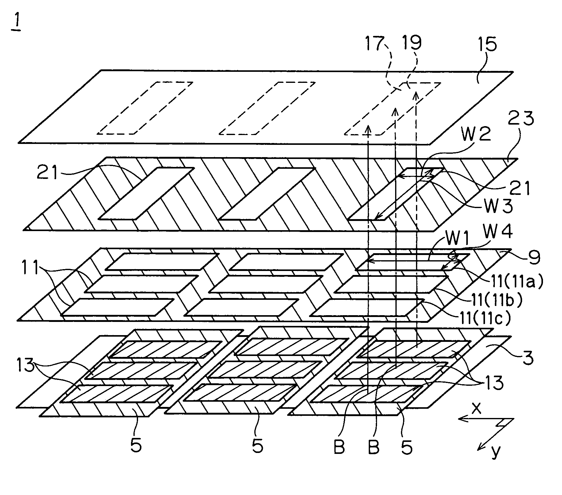
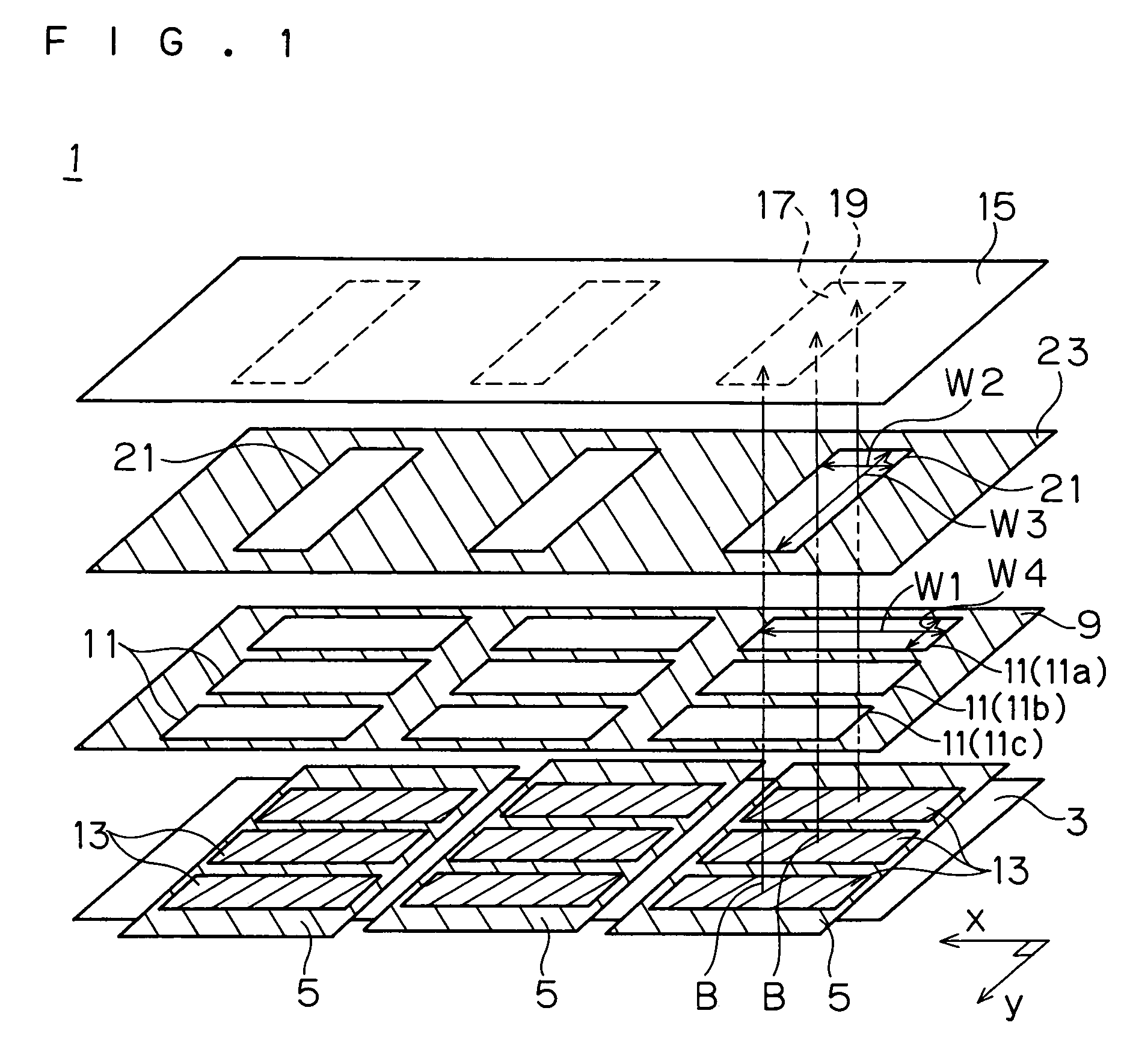
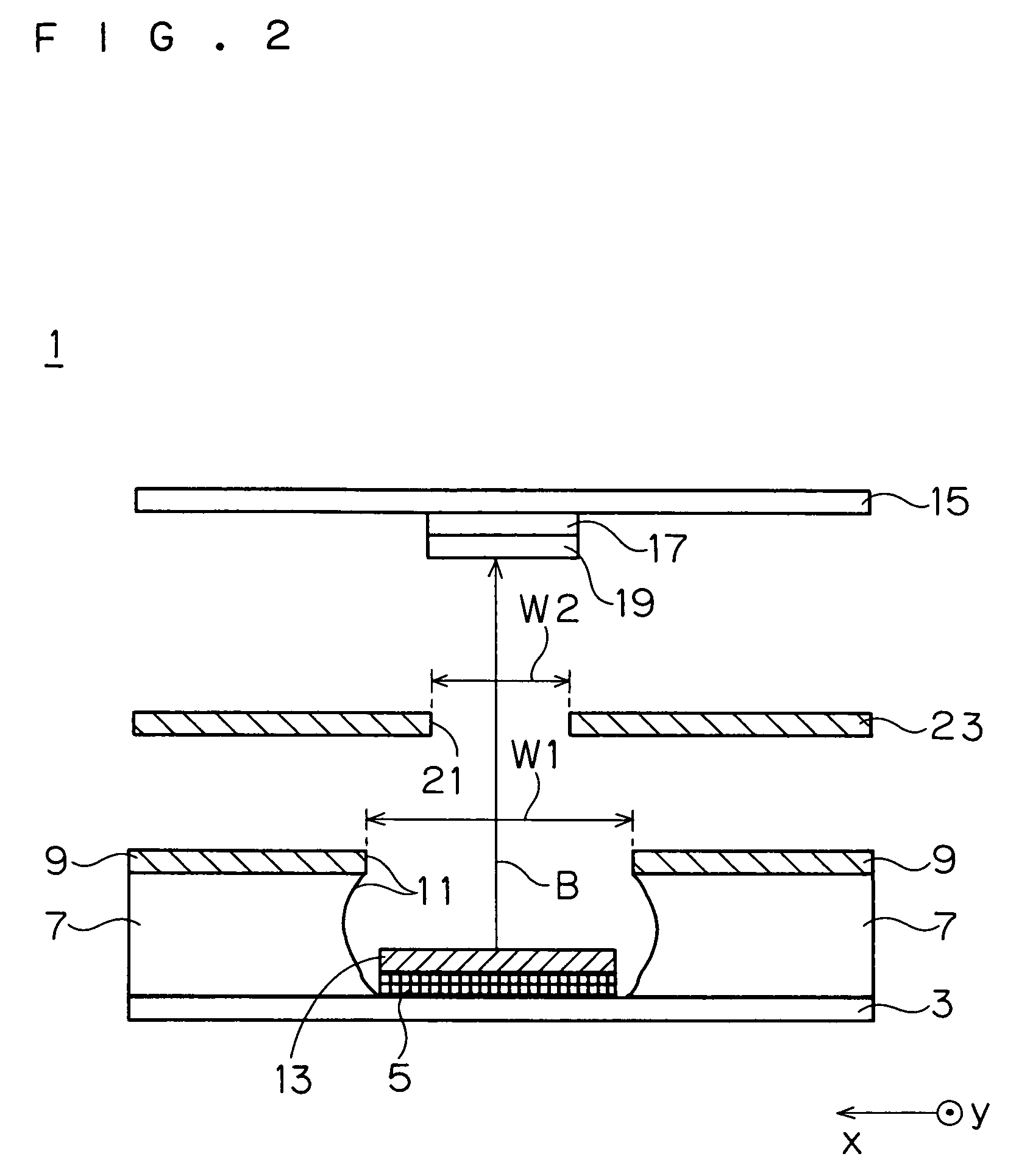
[0023]As shown in FIGS. 1 and 2, a field emission display device 1 according to this preferred embodiment of the present invention includes a cathode substrate 3, cathode electrodes 5 formed on the cathode substrate 3, flat electron emission material layers 13 formed on the cathode electrodes 5 and substantially similar in shape to, for example, openings 11 of a control electrode 9 to be described later, the control electrode 9 located at the front of the electron emission material layers 13 and having the openings 11 opposed to the electron emission material layers 13, a transparent anode substrate 15 located at the front of the control electrode 9, for example, transparent anode electrodes 17 formed on the rear surface of the anode substrate 15, phosphors 19 formed on the anode electrodes 17, and a shield electrode 23 located between the control electrode 9 and the anode electrodes 17 and formed with electron pass apertures 21 through which an electron beam B flowing from the elec...


PUM


Abstract

In a field emission display device, an opening dimension in a predetermined direction (or x direction) of an opening of a control electrode is greater than an opening dimension in the predetermined direction of an electron pass aperture of a shield electrode, and the shield electrode is located at the front of the control electrode so that the entire range of the opening dimension in the predetermined direction of the electron pass aperture is within the range of the opening dimension in the predetermined direction of the opening of the control electrode.

Description

BACKGROUND OF THE INVENTION[0001]1. Field of the Invention[0002]The present invention relates to a field emission display device capable of improving light emission uniformity of a phosphor surface (or display surface) of the field emission display device, and a method of manufacturing the same.[0003]2. Description of the Background Art[0004]In general, a field emission display device principally includes a cathode substrate formed with cathode electrodes, an insulating layer formed on the cathode substrate and the cathode electrodes, control electrodes formed on the insulating layer, electron emission material layers received in openings formed through the control electrodes and the insulating layer and formed on exposed portions of the cathode electrodes at the bottom of the openings, and an anode substrate located at the front of the control electrodes and formed with anode electrodes and phosphors (U.S. Pat. No. 3,500,102 (See FIGS. 1 to 4) and U.S. Pat. No. 4,857,799 (See FIGS....

Claims


Application Information

Patent Timeline
IPC IPC(8): H01J9/02H01J1/62H01J21/10H01J9/00H01J9/14H01J9/24H01J29/04H01J29/46H01J29/48H01J31/12H01J63/04
CPCH01J9/148H01J29/467H01J31/127H01J2329/4617H01J2329/4604
Inventor OONO, KATSUMI
Owner MITSUBISHI ELECTRIC CORP
Why Eureka
Try Eureka