

Image sensor package
a technology of image sensor and package, applied in the direction of instruments, optical elements, discharge tube/lamp details, etc., can solve the problems of inconvenient, even impossible, and achieve the effect of reducing the volume of the module and the manufacturing cost, and being convenient to be packaged
- Summary
- Abstract
- Description
- Claims
- Application Information
AI Technical Summary
Benefits of technology
Problems solved by technology
Method used
Image

Examples
Embodiment Construction
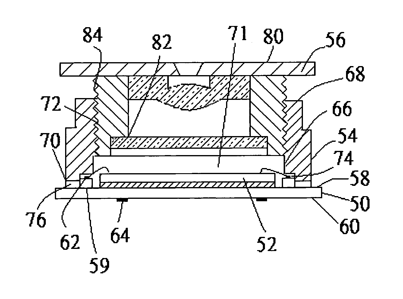
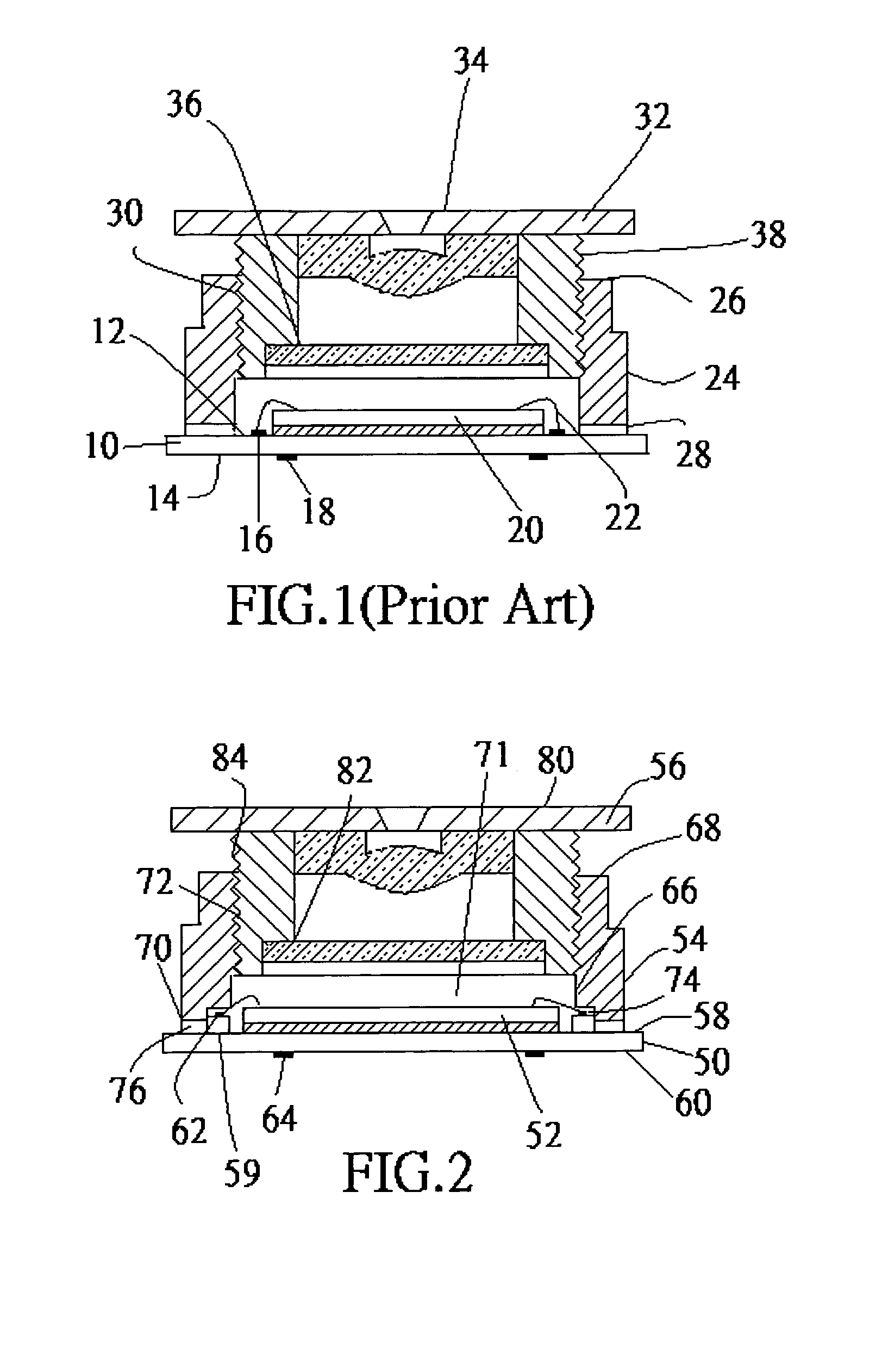
[0012]Please refer to FIG. 2 is an image sensor module of the present invention includes a substrate 50, a frame layer 59, a photosensitive chip 52, a lens holder 54, and a lens barrel 56.
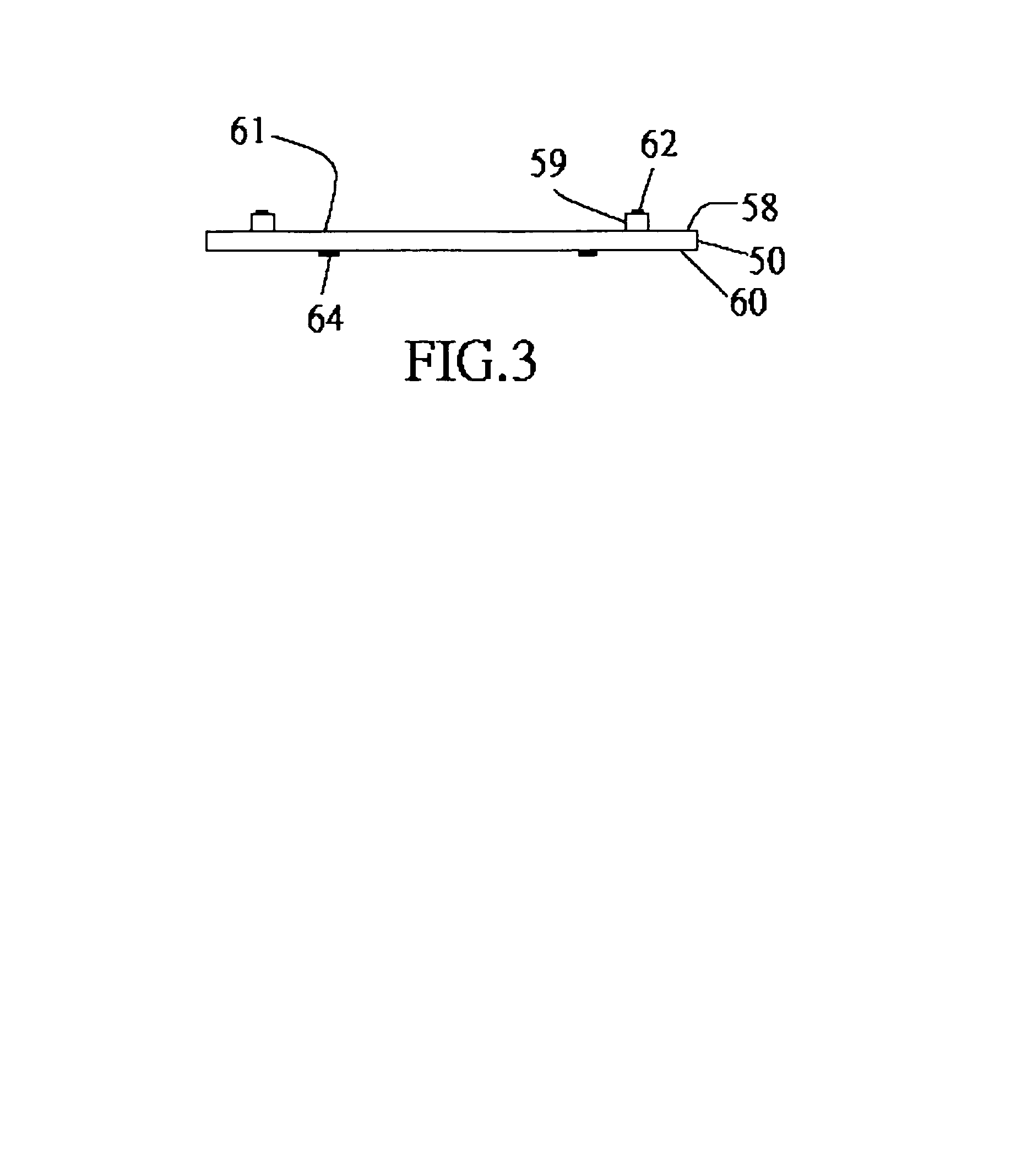
[0013]Please refer to FIG. 3. The substrate 50 has an upper surface 58 and a lower surface 60 on which a plurality of second electrodes 64 are formed.
[0014]The frame layer 59 is arranged on the upper surface 58 of the substrate 50, a cavity 61 is formed between the frame layer 59 and substrate 50, a plurality of first electrodes 62 are formed on the frame layer 59.
[0015]The photosensitive chip 52 is mounted on the upper surface 58 of the substrate 50, and is located within the cavity 61, then, the photosensitive chip 52 is electrically connected to the first electrodes 62 of the frame layer 59 by wires 66.
[0016]The lens holder 54 has an upper end face 68, a lower end face 70, and an opening 71 penetrating through the lens holder 54. The upper end of the opening 71 is formed with an internal thread ...
PUM
 Abstract
Description
Claims
Application Information