Imaging device with boosting circuit

a technology of boosting circuit and imaging device, which is applied in the direction of color television details, television systems, picture signal generators, etc., can solve the problems of increasing the activating speed of imaging devices, requiring a certain amount of time for the voltage supplied to a drive circuit,

Active Publication Date: 2007-12-18
SEMICON COMPONENTS IND LLC
View PDF9 Cites 165 Cited by
  • Summary
  • Abstract
  • Description
  • Claims
  • Application Information

AI Technical Summary

Problems solved by technology

As a result, a certain amount of time is required for the voltage supplied to a drive circuit to reach

Method used


Image

  • Imaging device with boosting circuit
  • Imaging device with boosting circuit
  • Imaging device with boosting circuit

Examples


first embodiment

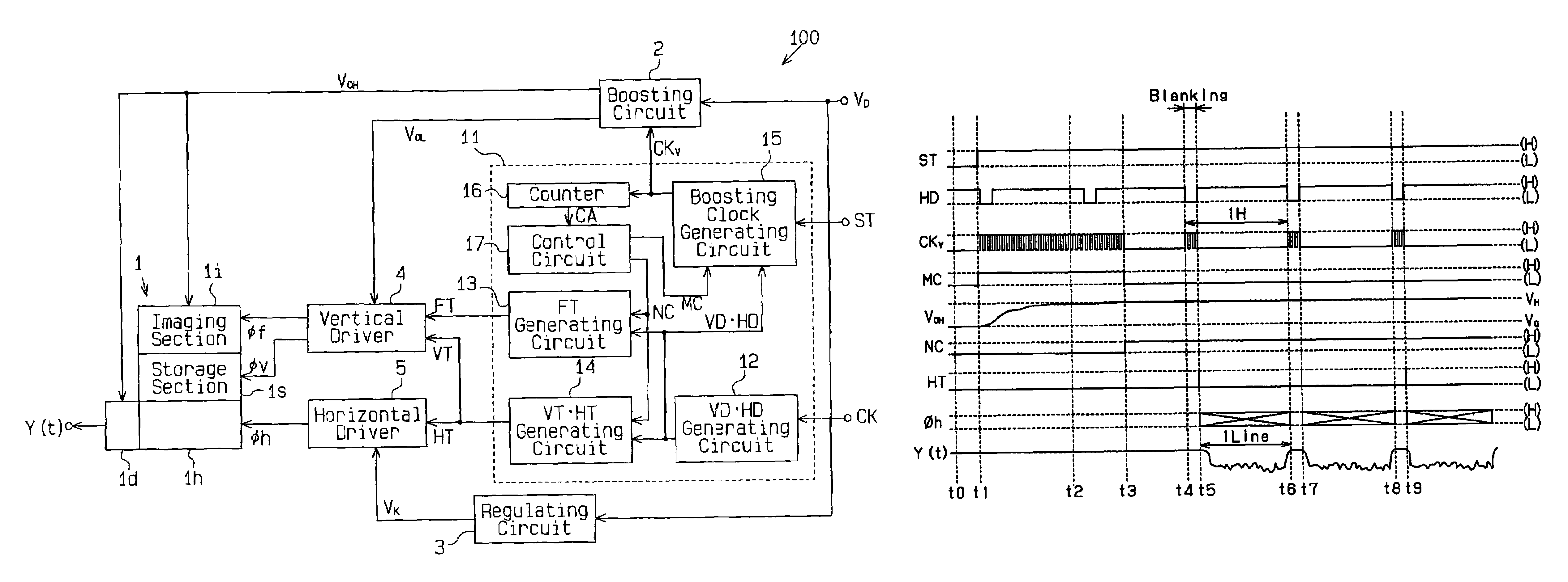
[0029]FIG. 3 is a schematic block diagram of an imaging device 100 according to the present invention. The imaging device 100 includes a CCD image sensor 1, a boosting circuit 2, a regulating circuit 3, a vertical driver circuit 4, a horizontal driver circuit 5, and a timing control unit 11, which is a clock signal generation unit.

[0030]In the first embodiment, a feature of the imaging device 100 is in that the boosting circuit 2 is continuously provided with the boosting clock signal CKV when the imaging operation is started. Further, modes for generating the boosting clock signal CKV are switched when the output voltage (boosted voltage) of the boosting circuit 2 increases to the required value.

[0031]The timing control unit 11 includes a VD / HD generation circuit 12, an FT generation circuit 13, a VT / HT generation circuit 14, a boosting clock signal generation circuit 15, a counter 16, and a control circuit 17.

[0032]The VD / HD generation circuit 12 includes a plurality of counters f...

second embodiment

[0056]In the second embodiment, the boosting operation of the boosting circuit 2 is positively performed from timing t1. After the boosted voltages VOH and VOL stabilize, boosting is performed only in the blanking period. This quickly increases the boosted voltage and prevents deterioration of the image signal.

[0057]In the second embodiment, the timing at which the positive boosted voltage VOH reaches the reference voltage VRH may differ from the timing at which the negative boosted voltage VOL reaches the reference voltage VOL. In such a case, the comparison signal KA goes low when the two boosted voltages VOH and VOL both reach the associated reference voltages VRH and VRL.

[0058]It should be apparent to those skilled in the art that the present invention may be embodied in many other specific forms without departing from the spirit or scope of the invention. Particularly, it should be understood that the present invention may be embodied in the following forms.

[0059]The boosting c...


PUM


Abstract

An imaging device that is activated quickly and prevents deterioration of an image signal. The imaging device includes a boosting circuit for boosting an input voltage to generate a boosted voltage. A solid state imaging device receives the boosted voltage and generates the image signal. A clock signal generation unit is connected to the boosting circuit to determine a timing for generating the image signal in correspondence with a vertical synchronization signal and a horizontal synchronization signal and to generate a boosting clock signal for operating the boosting circuit. The clock signal generation unit continuously generates the boosting clock signal during a predetermined period in which the imaging operation starts and, after the predetermined period, generates the boosting clock signal during at least part of a blanking period of the vertical synchronization signal and the horizontal synchronization signal.

Description

CROSS-REFERENCE TO RELATED APPLICATIONS[0001]This application is based upon and claims the benefit of priority from the prior Japanese Patent Application No. 2002-094745, filed on Mar. 29, 2002, the entire contents of which are incorporated herein by reference.BACKGROUND OF THE INVENTION[0002]The present invention relates to an imaging device incorporating a boosting circuit for generating a boosted voltage.[0003]Batteries are used as power supplies in imaging devices, such as digital cameras, that employ solid state imaging devices (CCD image sensors). A battery has a predetermined output voltage width. Thus, an imaging device is provided with a boosting circuit and a regulating circuit to drive the CCD image sensor.[0004]FIG. 1 is a schematic block diagram of a prior art imaging device 50. The imaging device 50 includes a CCD image sensor 1, a boosting circuit 2, a regulating circuit 3, a vertical driver circuit 4, a horizontal driver circuit 5, and a timing control circuit 6. In ...

Claims


Application Information

Patent Timeline
IPC IPC(8): H04N5/225H04N5/228H04N5/235H04N9/04H04N5/232H04N5/335H04N5/341H04N5/3725H04N5/376
CPCH04N5/23241H04N5/378H04N5/372H04N5/3698H04N23/651H04N25/709H04N25/71H04N25/70H04N25/75H02M3/07
Inventor TANIMOTO, TAKASHI
Owner SEMICON COMPONENTS IND LLC
Why Eureka
Try Eureka