Method and apparatus for in-situ film stack processing

a technology of in-situ film stack and processing method, which is applied in the direction of electrical equipment, electrical discharge tubes, decorative arts, etc., can solve the problems of high cost associated with tooling configured to process large area substrates, adverse effect of substrate transfer between tools, and high cost of transistor fabrication on large area substrates

Inactive Publication Date: 2008-04-15
APPLIED MATERIALS INC
View PDF58 Cites 171 Cited by
  • Summary
  • Abstract
  • Description
  • Claims
  • Application Information

AI Technical Summary

Problems solved by technology

Thus, the cost associated with tooling configured to process large area substrates continues to escalate dramatically.
As the metal etching, silicon etching, and deposition processes are typically performed in separate cluster tools, the cost for fabricating transistors on large area substrates is high due to the number and size of tools, and the additional expense of transferring the substrate between tools during processing.
Moreover, the number of substrate transfers between tools has an adverse effect on product yields due to the increase potential for contamination as the substrate is removed from the vacuum environment of one cluster tool for transfer to the next cluster tool required for the processing sequence.
Thus, the continued utilization of multiple tools for transistor fabrication is undesirable, particularly in light of the significant investment by the manufacturer represented in each large area substrate.

Method used


Image

  • Method and apparatus for in-situ film stack processing
  • Method and apparatus for in-situ film stack processing
  • Method and apparatus for in-situ film stack processing

Examples


Embodiment Construction

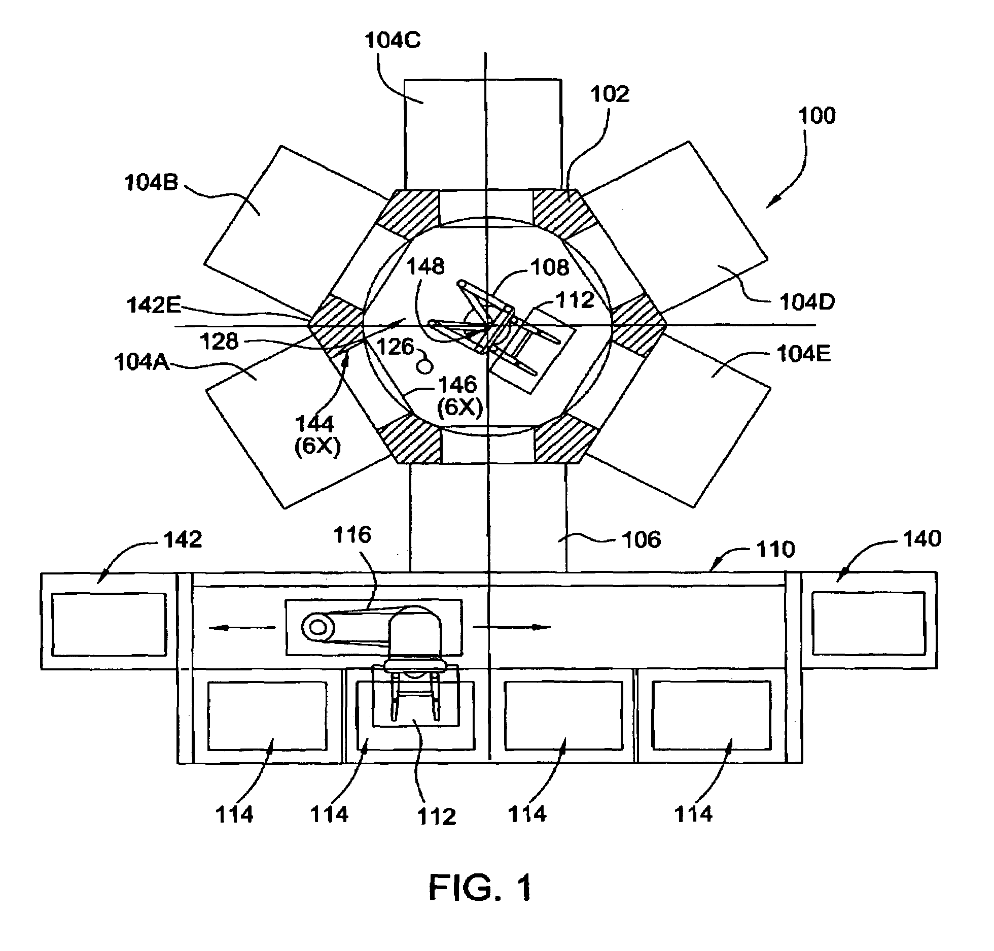
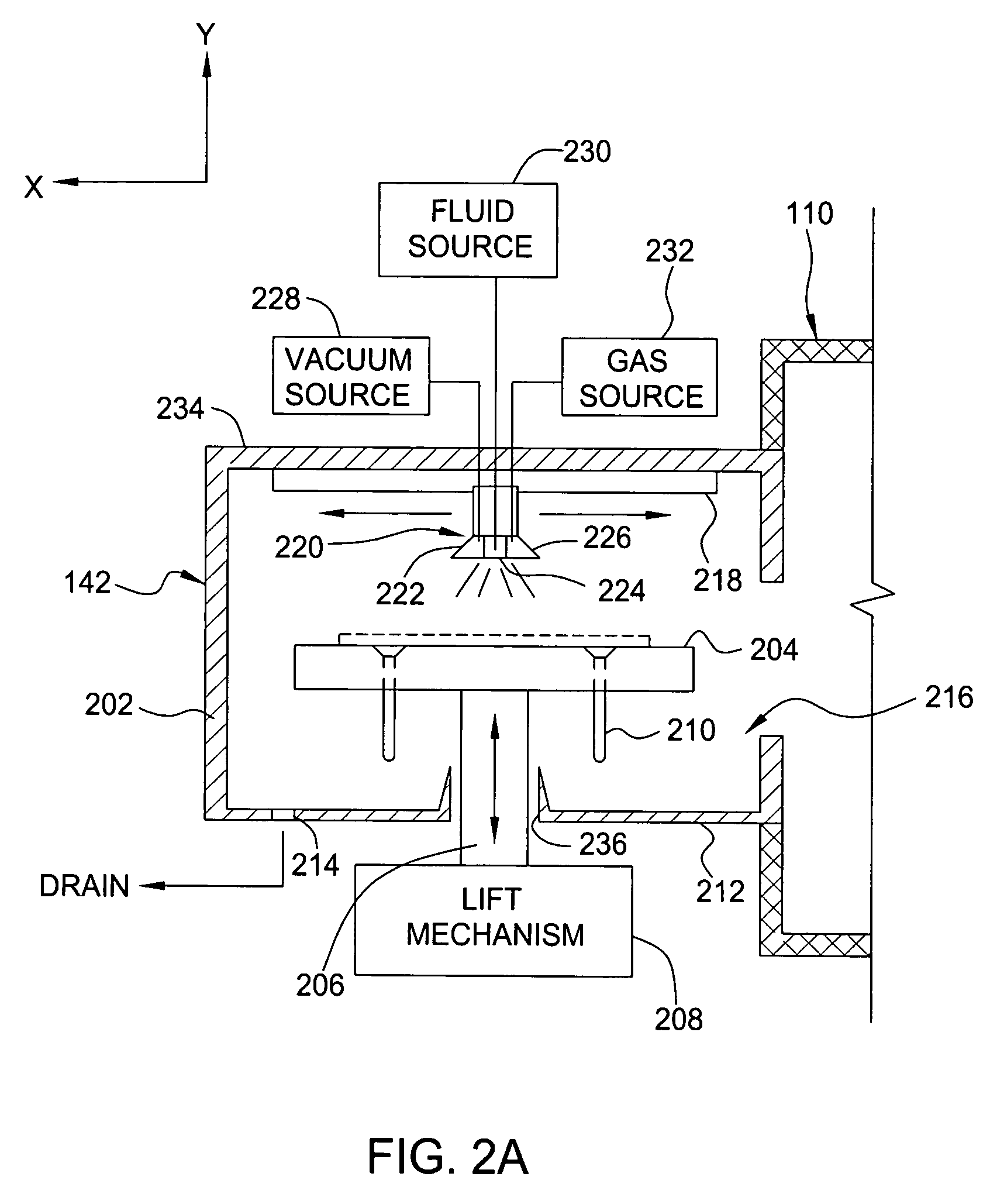
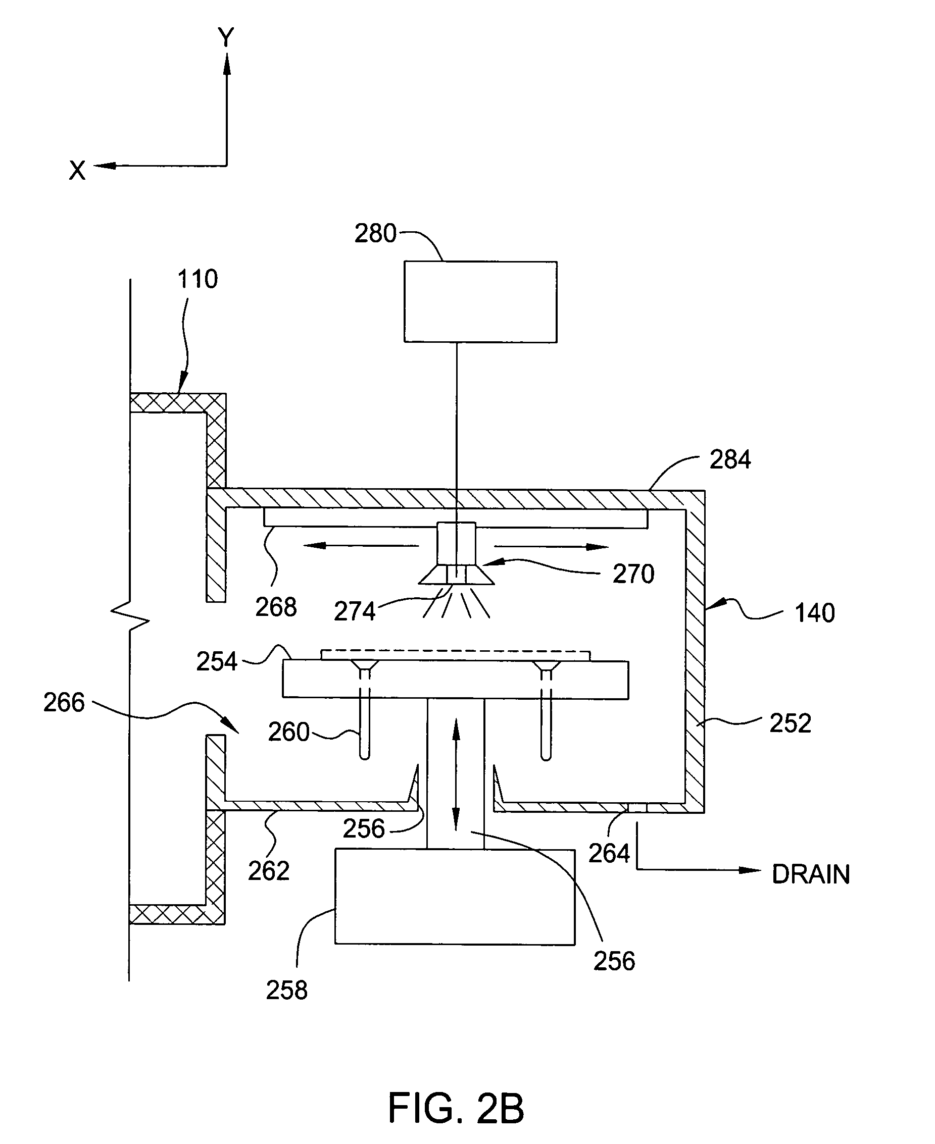
[0022]FIG. 1 depicts one embodiment of a semiconductor processing system or cluster tool 100 configured for in-situ processing of film stacks (i.e., without removal of the substrate from the tool) comprising different materials formed on large area substrates (e.g., substrates having a device side surface area of at least 0.25 square meters). The exemplary processing tool 100 generally includes a transfer chamber 102 circumscribed by one or more processing chambers 104A-E, a factory interface 110, one or more load lock chambers 106 and a post etch residual removal station 142. The processing tool 100 may optionally include a coating station 140. In the embodiment depicted in FIG. 1, one load lock chamber 106 is disposed between the transfer chamber 102 and the factory interface 110 to facilitate substrate transfer between a vacuum environment maintained in the transfer chamber 102 and a substantially ambient environment maintained in the factory interface 110. A transfer robot 108 i...


PUM

PropertyMeasurementUnit
areaaaaaaaaaaa
sizeaaaaaaaaaa
surface areaaaaaaaaaaa

Abstract

Embodiments of a cluster tool, processing chamber and method for processing a film stack are provided. In one embodiment, a method for in-situ etching of silicon and metal layers of a film stack is provided that includes the steps of etching an upper metal layer of the film stack in a processing chamber to expose a portion of an underlying silicon layer, and etching a trench in the silicon layer without removing the substrate from the processing chamber. The invention is particularly useful for thin film transistor fabrication for flat panel displays.

Description

BACKGROUND OF THE INVENTION[0001]1. Field of the Invention[0002]Embodiments of the invention generally relate to a method and apparatus for multilayer filmstack removal processing of metal and silicon materials in-situ. The invention is particularly useful for thin film transistor fabrication for flat panel displays.[0003]2. Background of the Related Art[0004]Substrate processing is typically performed by subjecting a substrate to a plurality of sequential processes to create devices, conductors and insulators on the substrate. Each of these processes is generally performed in a process chamber configured to perform a single step of the production process. A number of process chambers are typically coupled to a central transfer chamber that houses a robot to facilitate transfer of the substrate between the process chambers, thereby facilitating efficient completion of a sequence of processing steps in a processing platform. A processing platform having this configuration is generall...

Claims


Application Information

Patent Timeline
Patent Type & Authority Patents(United States)
IPC IPC(8): H01L21/02B44C1/22C23F1/00G02FH01J37/32H01L21/302
CPCH01J37/32357H01J37/3244H01J37/32788H01J37/32522H01J2237/334H01J2237/3325H01L21/205H01L21/67
Inventor MERRY, WALTER R.SHANG, QUANYUANWHITE, JOHN M.
Owner APPLIED MATERIALS INC
Why Eureka
Try Eureka