
Method for manufacturing ceramic green sheet and method for manufacturing electronic part using that ceramic green sheet
a technology of ceramic green sheets and green sheets, which is applied in the manufacture of capacitors, circuit masks, metallic pattern materials, etc., can solve the problems of inability to add a process of shaping them after they are formed, short-circuit or conduction failure, and unevenness, so as to improve the pattern shape of electrodes, improve the position, shape and thickness of electrodes, and eliminate run-over or sag of electrodes
- Summary
- Abstract
- Description
- Claims
- Application Information
AI Technical Summary
Benefits of technology
Problems solved by technology
Method used
Image

Examples
first embodiment
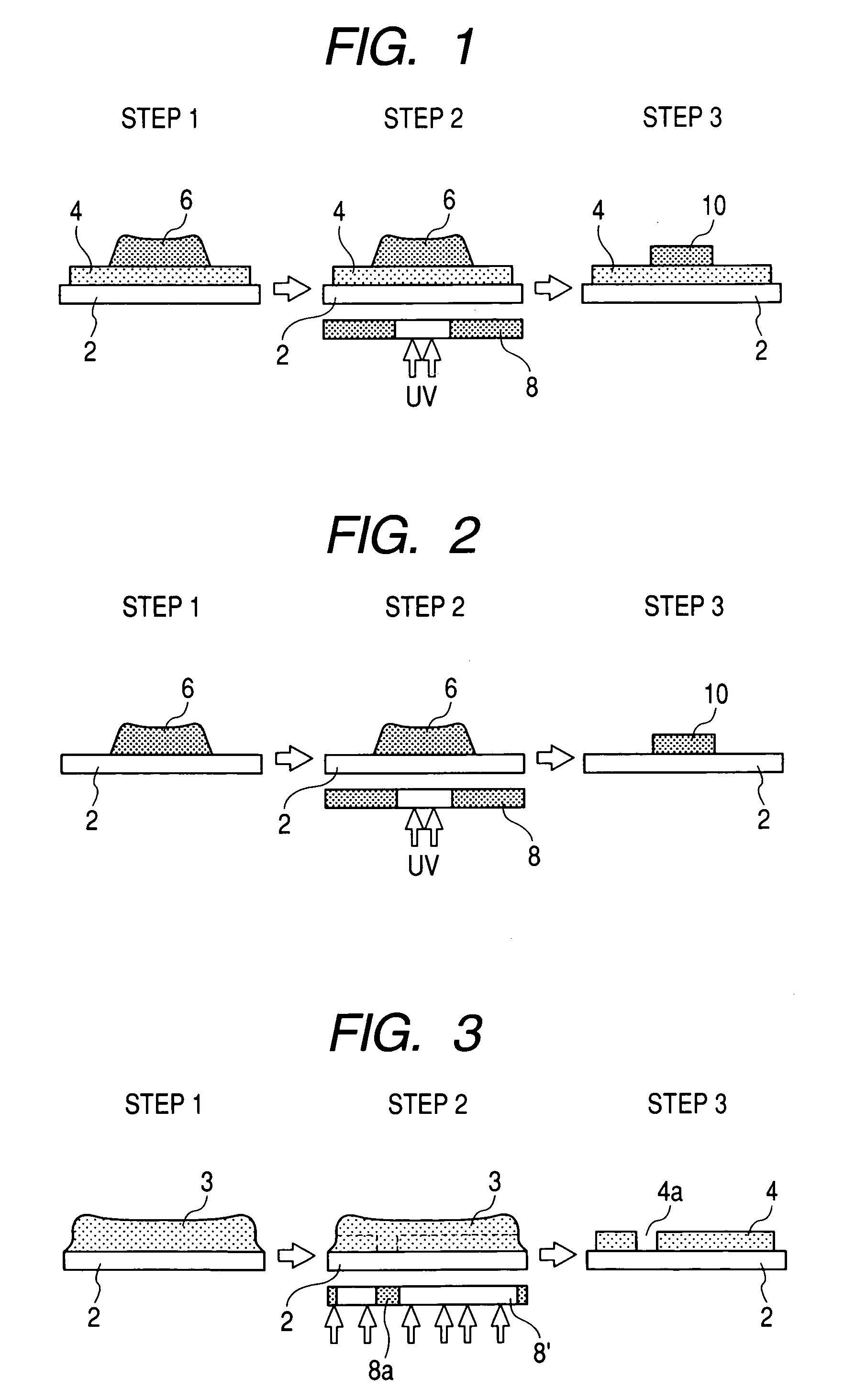
[0030]A layer forming method according to the first embodiment of the present invention is illustrated in FIG. 1. FIG. 1 shows the cross sectional structure of layers or a sheet taken along the thickness direction in various stages of the process. The method according to this embodiment is intended to form an electrode layer having a specific thickness and shape. In the method according to this embodiment, a photosensitive layer 6 for forming an electrode layer is applied on a member composed of a base member 2 made of a light transmissive film (e.g. a PET film) and a light transmissive insulating layer 4 formed thereon (step 1). Next, in step 2, a mask 8 having a desired pattern formed thereon is disposed in close contact with the back side surface of the base member 2, and ultraviolet radiation is applied from the back side thereof so that exposure of the photosensitive layer 6 is performed.
[0031]In connection with the present invention, the inventor discovered the fact that the d...
second embodiment
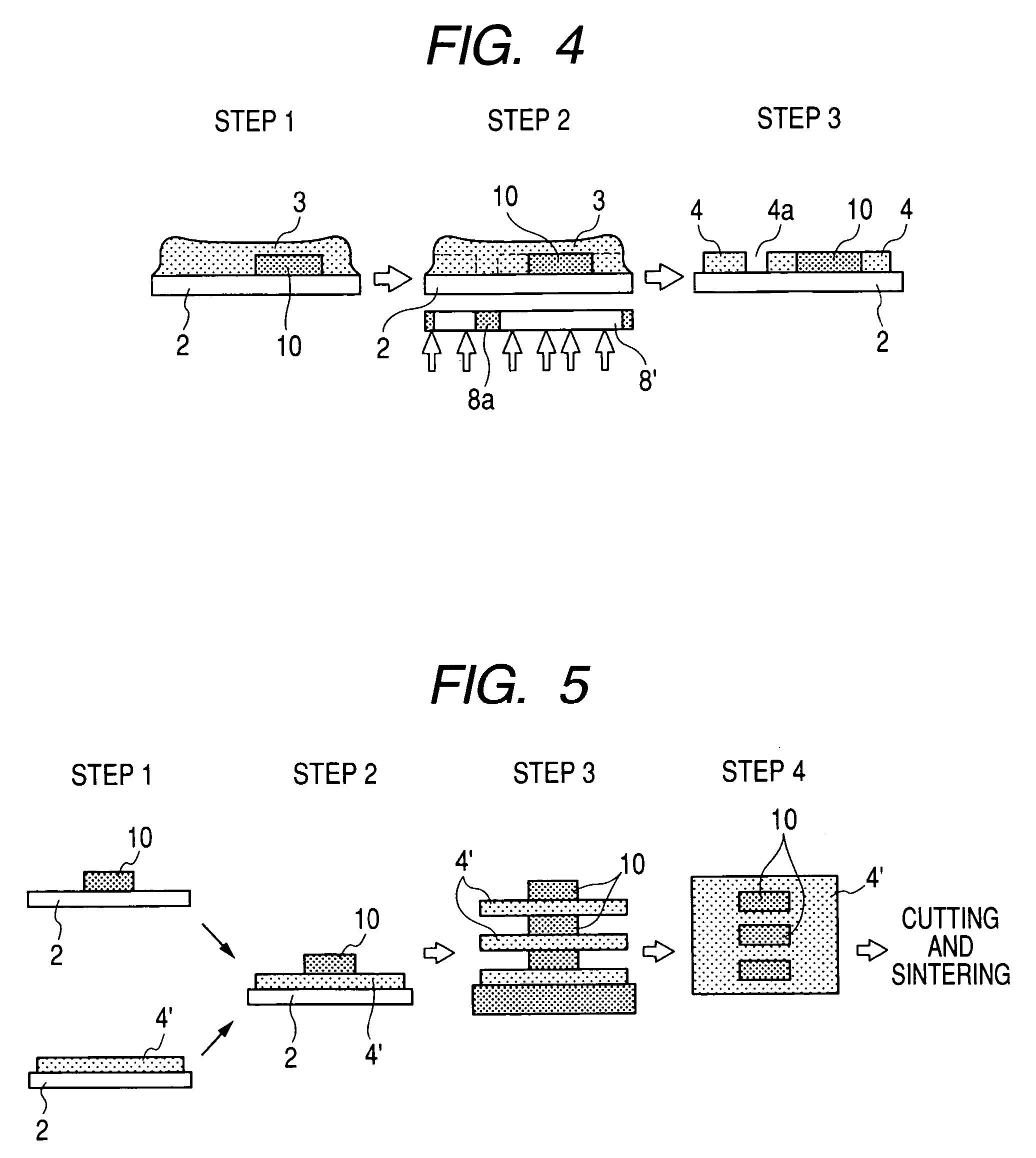
[0035]FIG. 2 is a diagram similar to FIG. 1, which shows the cross sectional structure of layers or a sheet taken along the thickness direction in various stages of the process. The other drawing that will be referred to in the following shall also show the cross sectional structure of the sheet in various stages of a process. In this embodiment, an electrode 10 is formed directly on a light transmissive base member 2. In other words, this embodiment is equivalent to the case that the insulating layer 4 or a layer corresponding to the insulating layer 4 is eliminated from the first embodiment.
[0036]Specifically, a photosensitive layer 6 for forming an electrode layer is firstly applied on the light transmissive base member 2 made of, for example, a PET film (step 1). Next in step 2, a mask 8 having a desired pattern formed thereon is disposed in close contact with the back side surface of the base member 2, and ultraviolet radiation is applied from the back side thereof so that expo...
third embodiment
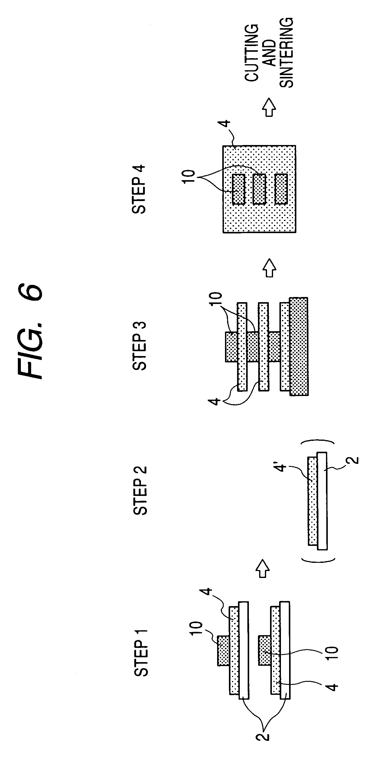
[0037]The method according to this embodiment is intended to form a through hole used upon forming a penetrating electrode simultaneously when, for example, an dielectric layer is formed. In the following, the layer forming method will be specifically described with reference to FIG. 3 which illustrates this embodiment. Firstly in step 1, a photosensitive layer 3 having desired electric characteristics is formed on the upper surface of a light transmissive base member 2 made of, for example, a PET film. Next in step 2, a mask 8′ having a desired pattern formed thereon is disposed in close contact with the back side surface of the base member 2, and ultraviolet radiation is applied from the back side thereof so that exposure of the photosensitive layer 3 is performed. After the exposure, development is performed so that the unexposed portion of the photosensitive layer corresponding to piercing pattern portion 8a is removed. Thus, a dielectric layer 4 having a through hole 4a is form...
PUM
| Property | Measurement | Unit |
|---|---|---|
| thickness | aaaaa | aaaaa |
| thickness | aaaaa | aaaaa |
| thickness | aaaaa | aaaaa |
Abstract
Description
Claims
Application Information