Method for manufacturing ceramic green sheet and method for manufacturing electronic part using that ceramic green sheet

a technology of ceramic green sheets and green sheets, which is applied in the direction of capacitor manufacturing, circuit masks, conductive pattern formation, etc., can solve the problems of inability to add a process of shaping them after they are formed, short-circuit or conduction failure, and unevenness, etc., to achieve excellent shape accuracy, improve quality, and thickness

Inactive Publication Date: 2005-04-14
TDK CORPARATION
View PDF5 Cites 7 Cited by
  • Summary
  • Abstract
  • Description
  • Claims
  • Application Information

AI Technical Summary

Benefits of technology

[0022] According to the present invention, a layer formed by a conventional process of applying a photosensitive material for example using a coater or screen printing is processed through exposure and development, so that variations in its position, shape and thickness can be reduced and formation of complex configuration having projections and recesses can be made possible. As a result, it is possible to produce a sheet used for forming multilayer electronic parts having improved quality as compared to conventional sheets only by adding the process according to the present invention to a conventional mass production process.
[0023] Furthermore, according to the present invention, it is possible to control the pattern shape, through hole formation and the layer thickness simultaneously. Consequently, in forming a layer including a pattern or a through hole etc., it is possible to shape or process the layer with excellent accuracy in its shape, thickness or other factors. Thus, it is possible to manufacture a preferable sheet to be used for manufacturing multilayer electronic parts having a shape closer to an ideal shape than in conventional methods. More specifically, it is possible to produce a sheet having a pattern width of about 30 μm with variations in thickness of ±2-3% or less.

Problems solved by technology

The thickness of the ceramic green sheets and the electrodes formed on the surface thereof, the width and pattern shape of the electrodes, are substantially determined at the time when they are formed, and it is practically impossible to add a process of shaping them after they are formed.
However, in the case that the layer to be exposed is formed by a printing process, there will be the aforementioned unevenness of the layer surface, and the unevenness will remain unchanged even when ordinary exposure and development processing has been applied.
However, it is not desirable because the process will become lengthy.
In addition, a run-over or faded portion can be generated upon application of slurry, which can cause short-circuit or conduction failure when assembled into an electronic part.
Furthermore, it is difficult to reduce variations in the dimension in the thickness direction down to less than a few percent.
However, at present, the thickness of the electrode is determined in accordance with the thickness of the ceramic sheet and it is practically difficult to control the thickness of the electrode independently from the thickness of the ceramic green sheet, as will be seen from Japanese Patent Application Laid-Open No. 2003-48303.
It is considered that screen printing can cope with this complexity with a measure of accuracy, but it is difficult to further improve the characteristics of the products as electronic parts.
In addition, it is difficult to attain desired cross sectional shape of the electrode or other parts.
However, it is impossible for conventional technologies to form such recesses with high accuracy.

Method used


Image

  • Method for manufacturing ceramic green sheet and method for manufacturing electronic part using that ceramic green sheet
  • Method for manufacturing ceramic green sheet and method for manufacturing electronic part using that ceramic green sheet
  • Method for manufacturing ceramic green sheet and method for manufacturing electronic part using that ceramic green sheet

Examples


first embodiment

[0035] (First Embodiment)

[0036] As described in the above general description of the embodiments, in the exposure process, the method of performing exposure with different light quantities for each area by using a simple light source and a mask may includes a method using a simple light source and a mask, a method of drawing a pattern using light having a significant intensity such as laser light, and a method of forming a pattern using an area light source in which a plurality of light sources are arranged. However, the process that is currently used most generally and considered to be most reliable is the process using a mask. Accordingly, a process using a mask will be described as an example.

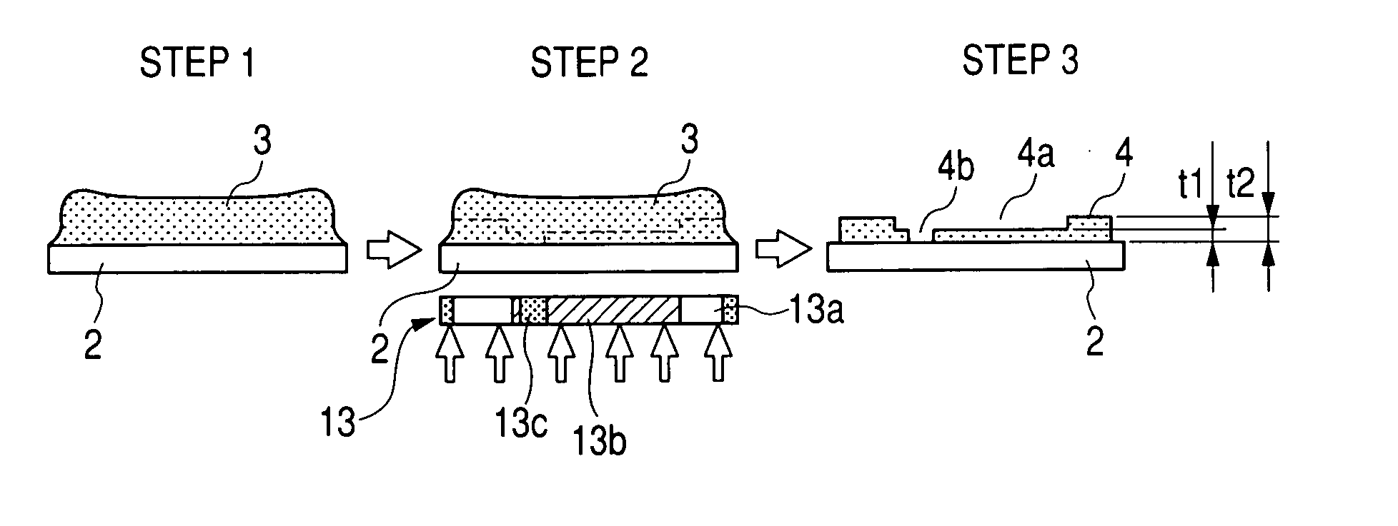
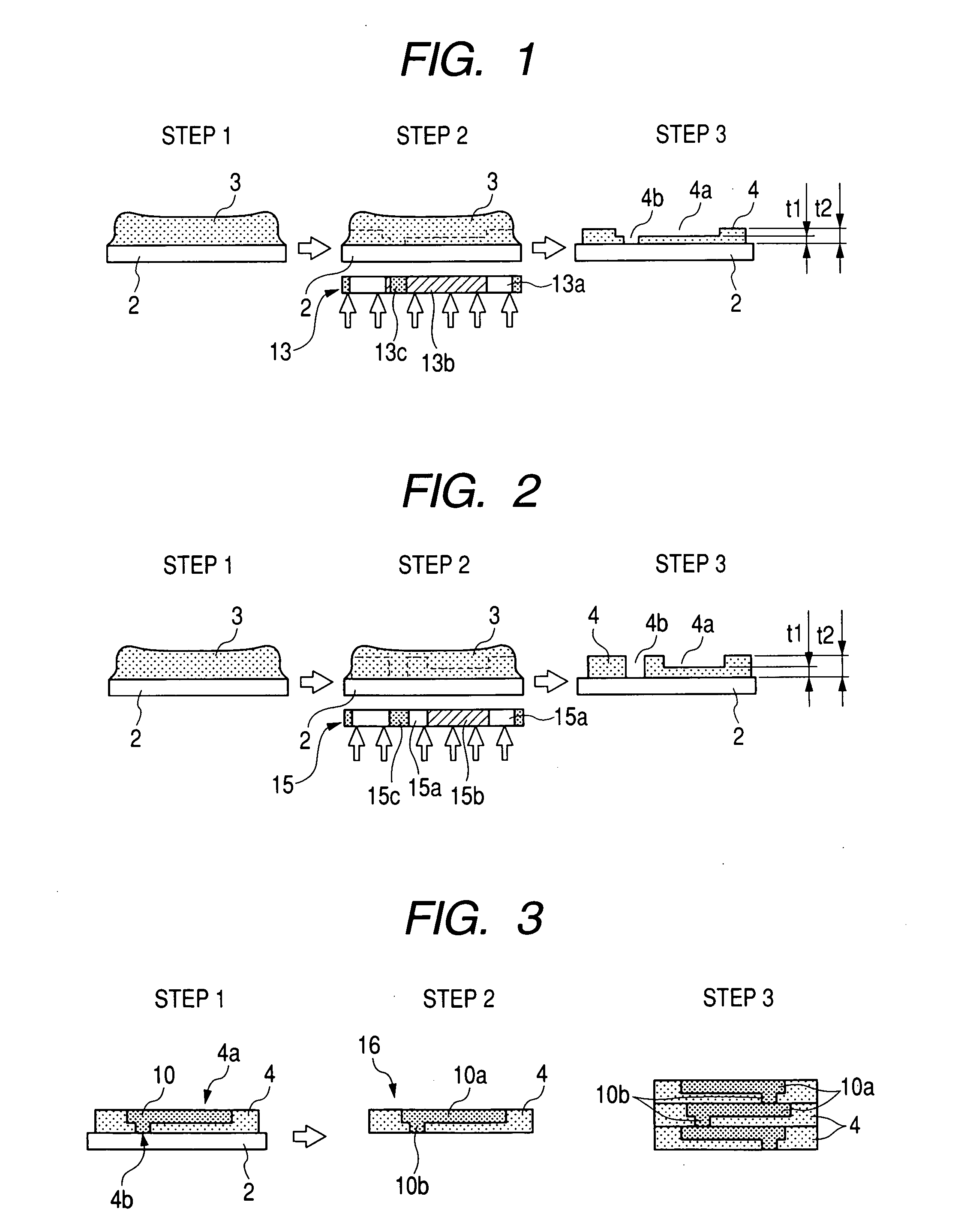
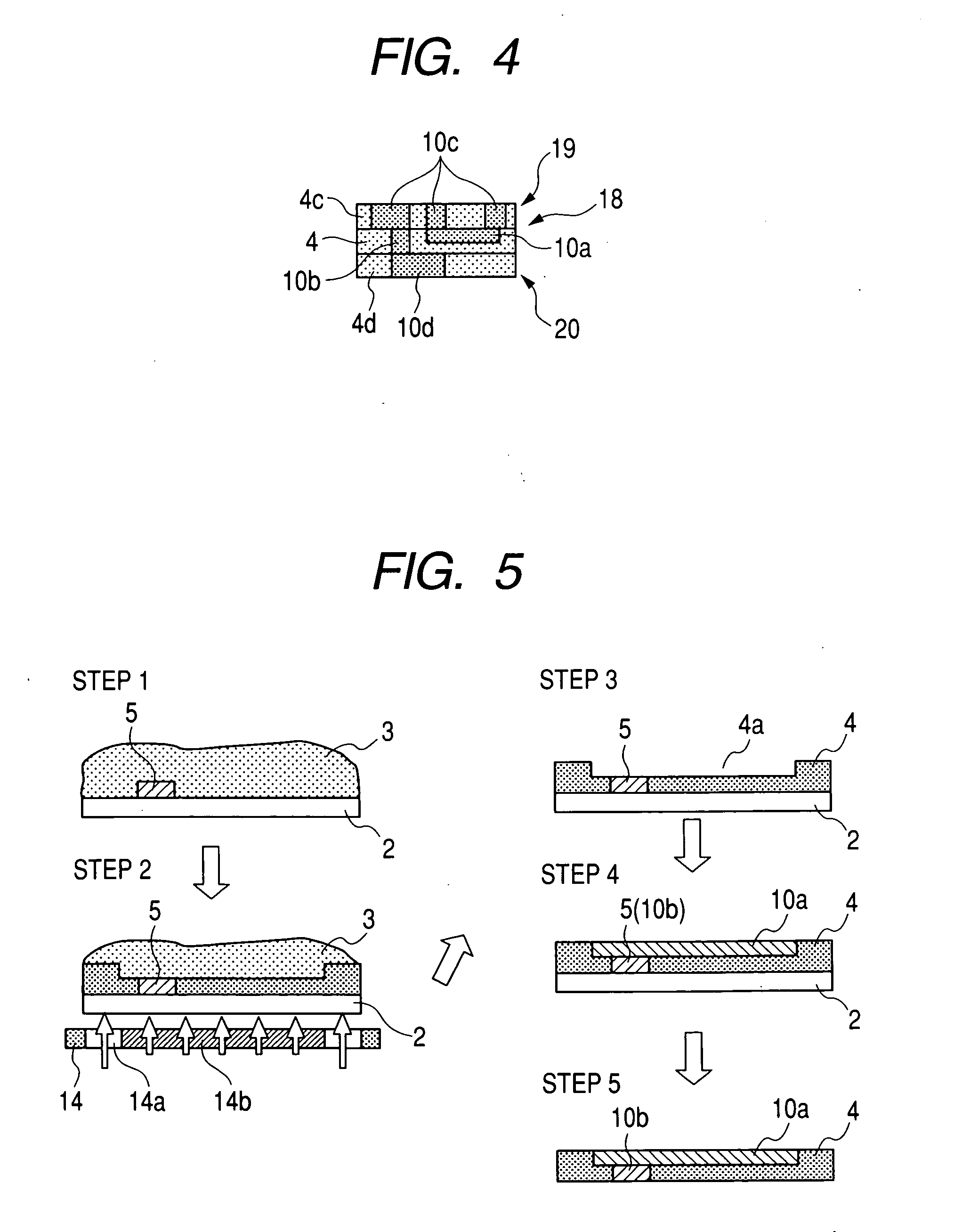
[0037]FIG. 1 shows a layer formation process according to the first embodiment of the present invention. FIG. 1 shows a cross sectional structure of layers or a sheet taken in the thickness direction in various stages of the process. In this embodiment, a photosensitive layer 3 containing p...

second embodiment

[0045] (Second Embodiment)

[0046]FIG. 2 is a diagram similar to FIG. 1, which shows a cross sectional structure of layers or a sheet taken along the thickness direction in various stages of the process. The other drawing that will be referred to in the following shall also show a cross sectional structure of the sheet in various stages of a process. This embodiment is directed to a case in which a through hole is formed in an insulating layer 4. Specifically, a photosensitive material 3 is applied on a base member 2 made of a PET film (step 1). Next in step 2, a mask 15 in which a desired electrode pattern 15b and a through hole pattern 15c are separately formed is disposed in close contact with the back side surface of the base member 2, and ultraviolet radiation is applied from the back side thereof.

[0047] In this process, the exposure amount is controlled so that the thickness of the cured portion of the photosensitive layer 3 will be t1. The transmittance for ultraviolet light o...


PUM

PropertyMeasurementUnit
thicknessaaaaaaaaaa
thicknessaaaaaaaaaa
thicknessaaaaaaaaaa

Abstract

There is provided a sheet used for manufacturing multilayer electronic parts in which accuracy in shape and formation position and uniformity in thickness of a complex configuration with recesses and projections of an insulating layer or the like are assured. A layer made of a photosensitive material containing a powder having a specific electric characteristic is formed on a light transmissive base member. A mask having a plurality of patterns with different transmittances for ultraviolet light is disposed on the back side of the base member. The photosensitive material is subjected to an exposure process in which it is irradiated with ultraviolet light or the like through the mask. The photosensitive material is subjected to development process after the exposure process.

Description

BACKGROUND OF THE INVENTION [0001] 1. Field of the Invention [0002] The present invention relates to a method for manufacturing an electronic part, especially an electronic part that is formed by laminating ceramic layers, which is exemplified by a so-called multilayer ceramic electronic part. The present invention also relates to a method for manufacturing a so-called ceramic green sheet used in the aforementioned method. Examples of the multiplayer electronic part mentioned here include multilayer ceramic capacitors, multilayer ceramic inductors, LC composite parts including capacitors and inductors formed therein, or EMC related parts etc. [0003] 2. Related Background Art [0004] In recent years, with downsizing and rapid popularization of electronic apparatuses represented by cellular phones, an increase in mounting density of the electronic parts used for those apparatuses and improvement in their performance are required. Especially, demands for downsizing, decrease in thicknes...

Claims


Application Information

Patent Timeline
Patent Type & Authority Applications(United States)
IPC IPC(8): G03F7/00H01F41/00G03F7/20H01F17/00H01F41/34H01G4/12H01G4/30H01G13/00H05K1/03H05K3/00H05K3/10H05K3/12H05K3/46
CPCG03F7/20H05K1/0306H05K3/0023H05K3/0082H05K3/107H05K2203/0514H05K3/4614H05K3/4629H05K2201/0108H05K2201/09036H05K2203/016H05K3/1258H01F41/34H01G4/30H01G4/12
Inventor YOSHIDA, MASAYUKISUTOH, JUNICHIAOKI, SHUNJIWATANABE, GENICHI
Owner TDK CORPARATION
Why Eureka
Try Eureka