Technique for boron implantation

a technology of boron and boron atoms, which is applied in the field of boron implantation technology, can solve the problems of introducing unwanted contaminants, adversely affecting the process, and unable to provide diborane in its pure sta

Inactive Publication Date: 2008-07-08
VARIAN SEMICON EQUIP ASSOC INC
View PDF17 Cites 25 Cited by
  • Summary
  • Abstract
  • Description
  • Claims
  • Application Information

AI Technical Summary

Problems solved by technology

Due to safety and stability problems, diborane cannot be provided in its pure state.
When such diluted diborane is used for plasma immersion ion implantation, the carrier (diluent) gas molecules can become ionized and get implanted in addition to the boron-bearing species, thereby adversely impacting the process by complicating dosimetry, introducing unwanted contaminants, and imposing process space limitations on the implant process.

Method used


Image

  • Technique for boron implantation
  • Technique for boron implantation
  • Technique for boron implantation

Examples


Embodiment Construction

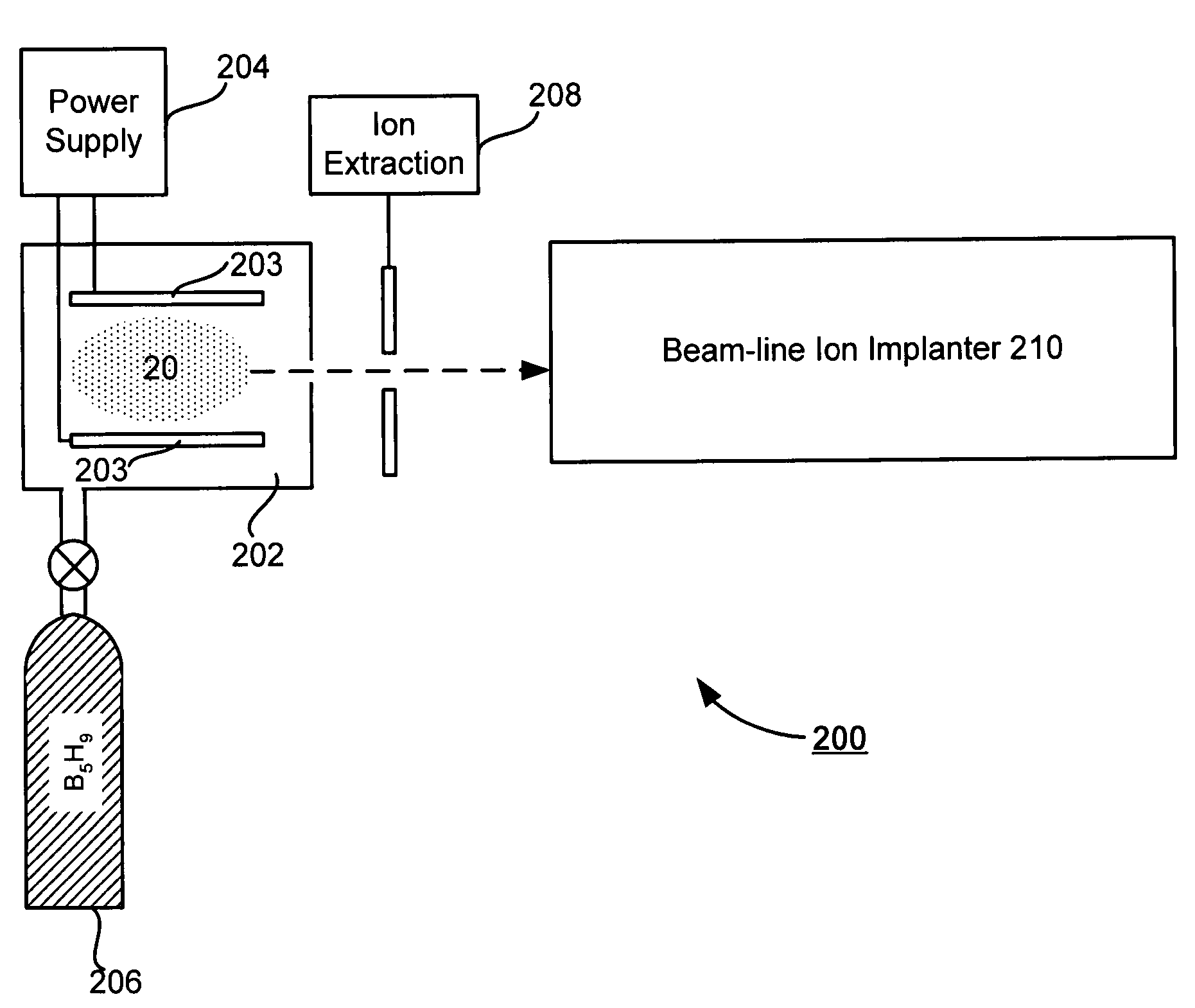
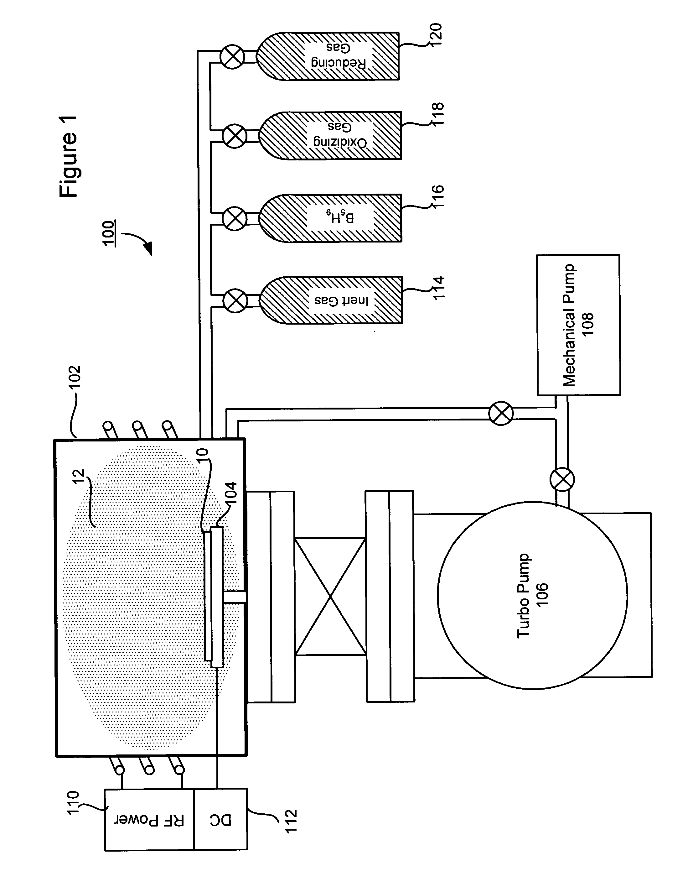
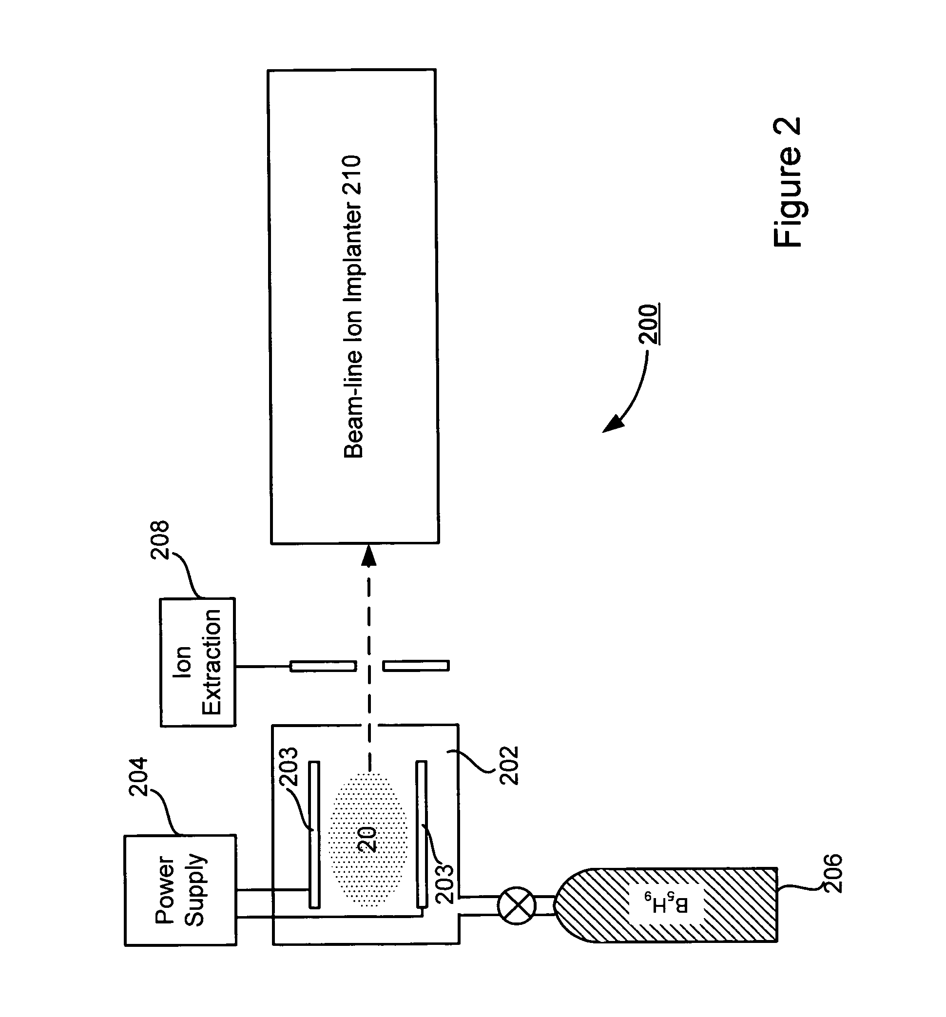
[0026]Embodiments of the present disclosure improve boron implantation by replacing the traditionally used diluted diborane (B2H6) with undiluted or substantially pure pentaborane (B5H9). In a plasma immersion ion implantation system or a beam-line ion implanter, a plasma discharge may be produced by energizing a gas containing a substantially pure form of pentaborane. Boron-bearing species generated in the plasma discharge may be implanted into a target wafer.

[0027]Use of a pure form of pentaborane offers a number of advantages. For example, unwanted co-implantation of diluent species may be reduced or avoided. In a pentaborane plasma, boron-bearing species of different masses are available for implantation, which allows shallower implants at a given voltage. Further, with pure pentaborane, there is a greater flexibility in process space parameters such as operating pressure, mass flow rate, and / or intentionally-added diluents.

[0028]Referring to FIG. 1, there is shown a block diagr...


PUM


Abstract

A technique for boron implantation is disclosed. In one particular exemplary embodiment, the technique may be realized by an apparatus for boron implantation. The apparatus may comprise a reaction chamber. The apparatus may also comprise a source of pentaborane coupled to the reaction chamber, wherein the source is capable of supplying a substantially pure form of pentaborane into the reaction chamber. The apparatus may further comprise a power supply that is configured to energize the pentaborane in the reaction chamber sufficiently to produce a plasma discharge having boron-bearing ions.

Description

CROSS-REFERENCE TO RELATED APPLICATIONS[0001]This patent application claims priority to U.S. Provisional Patent Application No. 60 / 611,065, filed Sep. 17, 2004, which is hereby incorporated by reference herein in its entirety.FIELD OF THE DISCLOSURE[0002]The present disclosure relates generally to semiconductor manufacturing and, more particularly, to a technique for boron implantation.BACKGROUND OF THE DISCLOSURE[0003]Ion implantation is a standard technique for introducing conductivity-altering dopant materials into semiconductor wafers. In a conventional (beam-line type) ion implantation system, a desired dopant material is ionized in an ion source, the ions are accelerated to form an ion beam of a prescribed energy, and the ion beam is directed at a semiconductor wafer. The energetic ions in the beam penetrate into the bulk of the semiconductor material and are embedded into the crystalline lattice of the semiconductor material.[0004]Compared with the traditional beam-line impla...

Claims


Application Information

Patent Timeline
Patent Type & Authority Patents(United States)
IPC IPC(8): H05H1/42
CPCH01J37/32082H01L21/26513H01L21/2236H01J37/32412
Inventor SINGH, VIKRAMWINDER, EDMUND J.PERSING, HAROLD M.MILLER, TIMOTHY JEROMEFANG, ZIWEIGUPTA, ATUL
Owner VARIAN SEMICON EQUIP ASSOC INC
Why Eureka
Try Eureka