

Data input buffer in semiconductor device
a data input buffer and semiconductor technology, applied in pulse manipulation, pulse technique, instruments, etc., can solve the problems of low current driving capability, and inconvenient data input buffer operation, so as to avoid the deterioration of the operation speed of the data input buffer
- Summary
- Abstract
- Description
- Claims
- Application Information
AI Technical Summary
Benefits of technology
Problems solved by technology
Method used
Image

Examples
Embodiment Construction
[0023]In accordance with the present invention, current driving capability of a data input buffer is adjusted by using sensing result that is obtained with a temperature sensor and / or process characteristic sensor. For this purpose, the present invention applies an element for adjusting current amount flowing through a data input part and a reference voltage input part step by step, and an element for making a current control signal from the sensing result. With the present invention, even under worst-case process characteristic or high temperature condition, operation speed deterioration of the data input buffer can be avoided.
[0024]Hereinafter, a data input buffer in a semiconductor device in accordance with the present invention will be described in detail referring to the accompanying drawings.
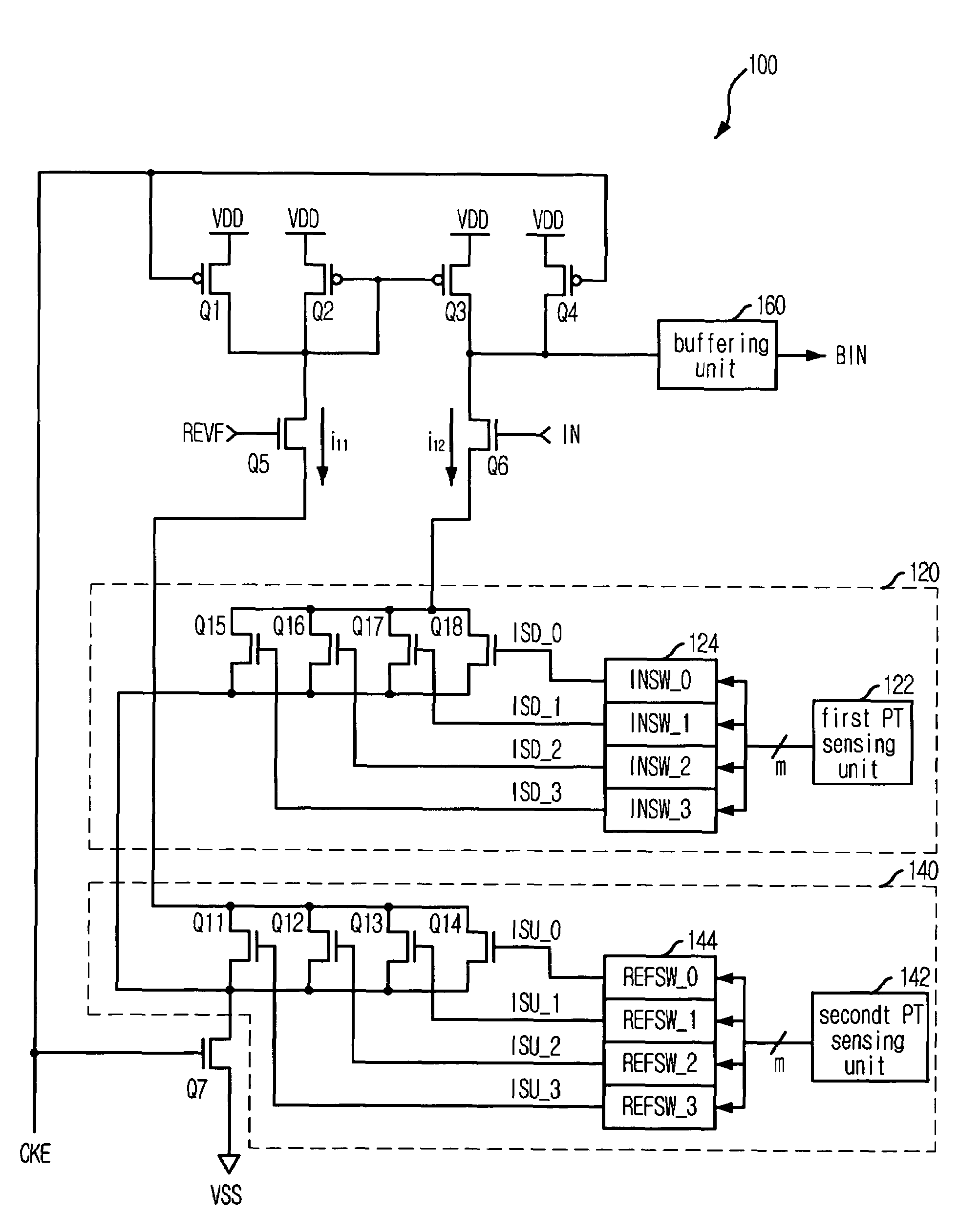
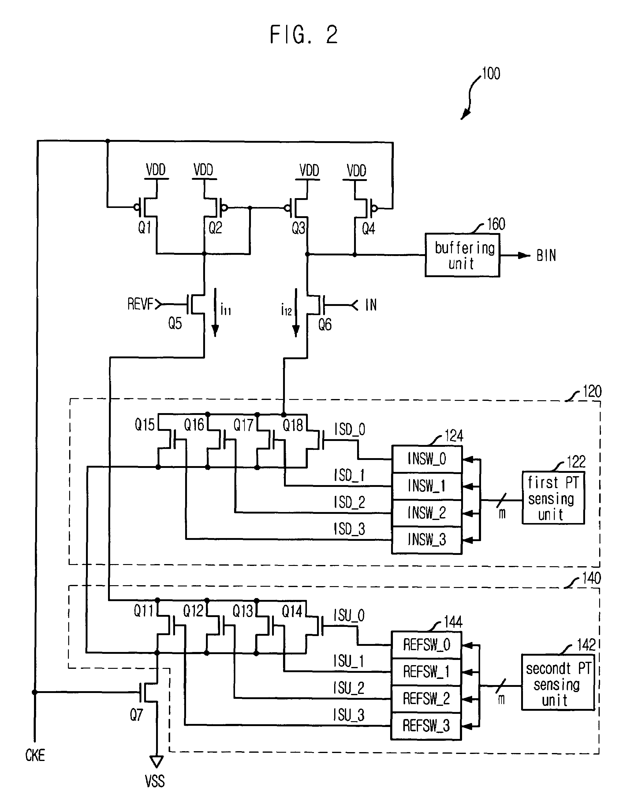
[0025]FIG. 2 provides a circuit diagram of a data input buffer in accordance with one embodiment of the present invention.
[0026]Referring to FIG. 2, the data input buffer 100 of the embodi...
PUM
 Abstract
Description
Claims
Application Information