Methods and apparatus for EMI shielding in multi-chip modules

a multi-chip module and electromagnetic shielding technology, applied in the direction of cross-talk/noise/interference reduction, printed circuit aspects, rigid plastic container screening, etc., can solve the problems of increasing the size of the component, and increasing the size of the semiconductor devi

Inactive Publication Date: 2010-01-19
TAIWAN SEMICON MFG CO LTD
View PDF16 Cites 59 Cited by
  • Summary
  • Abstract
  • Description
  • Claims
  • Application Information

AI Technical Summary

Problems solved by technology

Semiconductor devices continue to decrease in size and increase in power-density, resulting in a number of challenges for system designers.
One of the primary challenges relates to electromagnetic interference (EMI)—i.e., how to shield the internal components from each other as well as from external sources.
However, such solutions tend to increase the size of the component, and generally require additional processing steps and cost.

Method used


Image

  • Methods and apparatus for EMI shielding in multi-chip modules
  • Methods and apparatus for EMI shielding in multi-chip modules
  • Methods and apparatus for EMI shielding in multi-chip modules

Examples


Embodiment Construction

[0009]The following detailed description is merely exemplary in nature and is not intended to limit the invention or the application and uses of the invention. Furthermore, there is no intention to be bound by any expressed or implied theory presented in the preceding technical field, background, or the following detailed description. For the sake of brevity, conventional techniques related to semiconductor processing, electronic packaging, and device assembly are not described herein.

[0010]For simplicity and clarity of illustration, the drawing figures depict the general structure and / or manner of construction of the various embodiments. Descriptions and details of well-known features and techniques may be omitted to avoid unnecessarily obscuring other features. Elements in the drawings figures are not necessarily drawn to scale: the dimensions of some features may be exaggerated relative to other elements to assist improve understanding of the example embodiments.

[0011]Terms of en...


PUM


Abstract

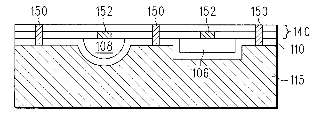
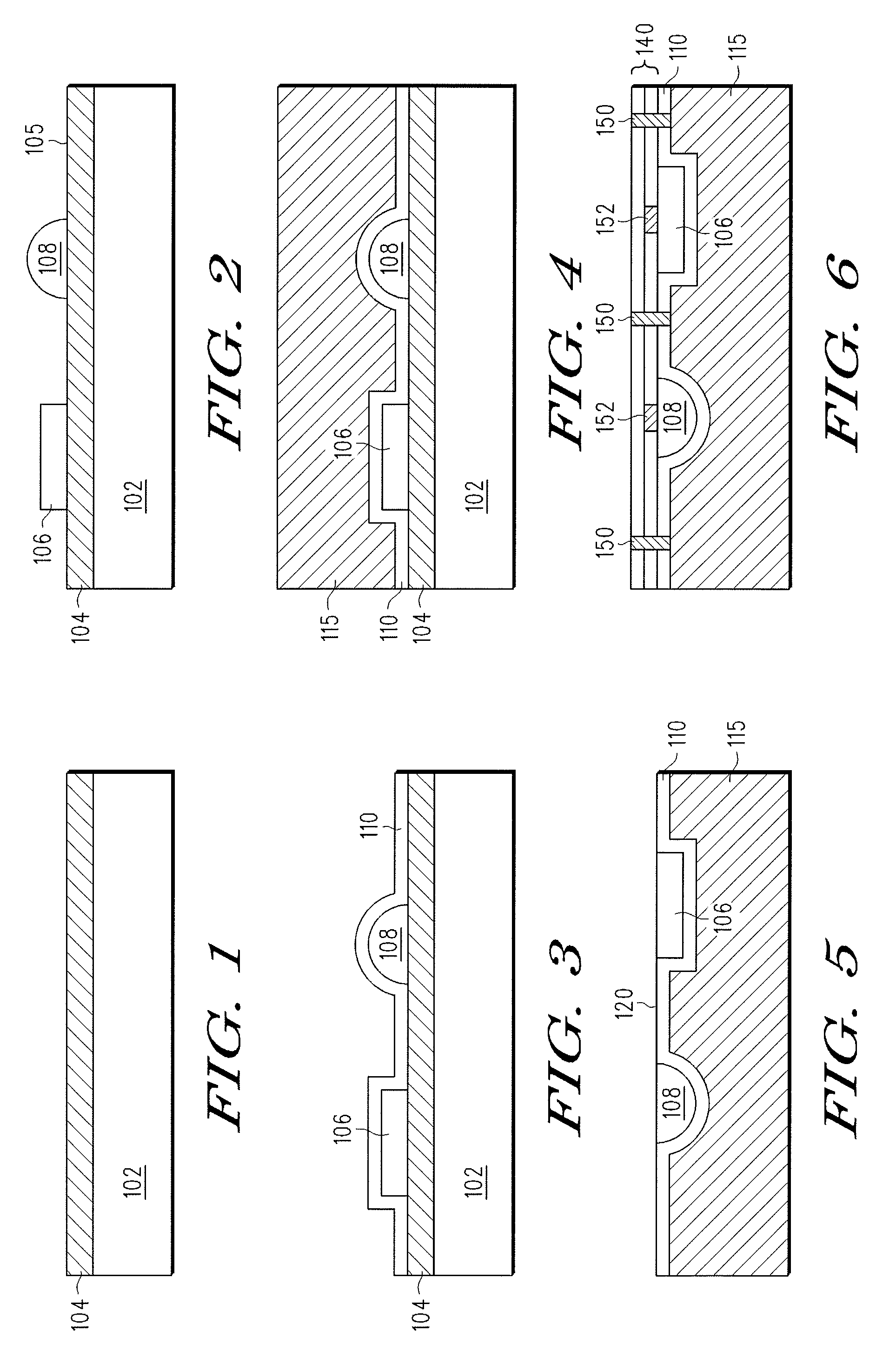
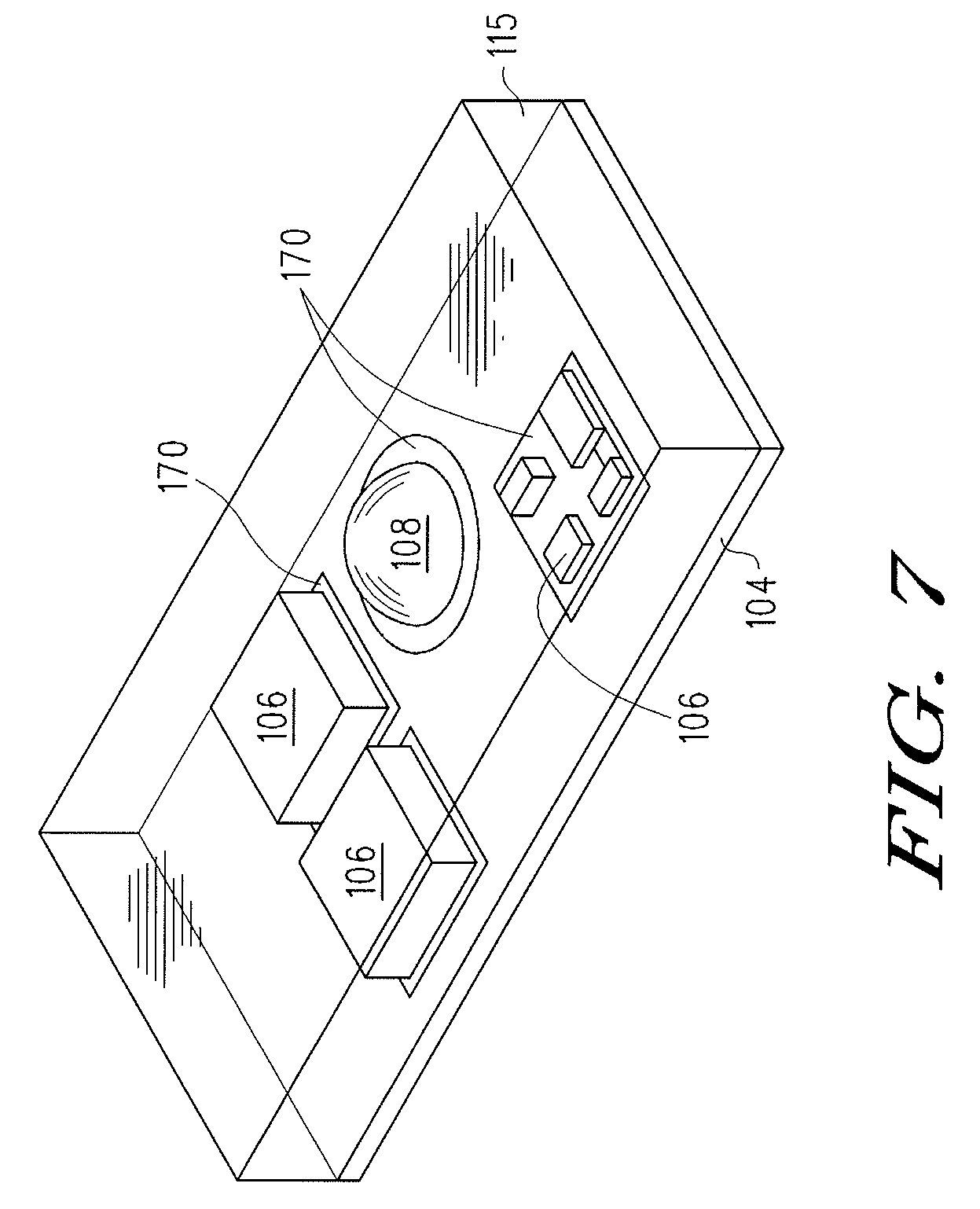
Methods and structures provide a shielded multi-layer package for use with multi-chip modules and the like. A substrate (102) (e.g., chip carrier) has an adhesive layer (104), where electronic components (106, 108) are attached. An insulating layer (110) is formed over the plurality of electronic components, and a conductive encapsulant structure (115) is formed over the insulating layer. The adhesive layer is detached from the electronic components, and multi-layer circuitry (140) is formed over, and in electrical communication with, the plurality of electronic components. A shielding via (150) is formed through the multilayer circuitry such that it contacts the conductive encapsulant.

Description

FIELD OF THE INVENTION[0001]The present invention generally relates to semiconductor assemblies and, more particularly, to methods of providing electromagnetic shielding for multi-chip modules and related packages.BACKGROUND OF THE INVENTION[0002]Semiconductor devices continue to decrease in size and increase in power-density, resulting in a number of challenges for system designers. One of the primary challenges relates to electromagnetic interference (EMI)—i.e., how to shield the internal components from each other as well as from external sources. Such shielding is particularly important in the context of multi-chip and multi-module RF integration.[0003]Chip-to-chip and module-to-module shielding is often provided using an embedded shield structure, a metal can cover, conformal shielding structures, or the like. However, such solutions tend to increase the size of the component, and generally require additional processing steps and cost.[0004]Accordingly, there is a need for high...

Claims


Application Information

Patent Timeline
Patent Type & Authority Patents(United States)
IPC IPC(8): H01L21/00H01L23/053H01L23/12H01L23/552
CPCH01L23/29H01L23/552H01L25/165H05K1/0218H01L24/97H05K9/0047H05K3/4644H05K2201/0215H05K2203/1316H05K1/185H01L2924/181H01L2924/00
Inventor TANG, JINBANGLIN, JONG-KAI
Owner TAIWAN SEMICON MFG CO LTD
Why Eureka
Try Eureka