

Methods and apparatuses for pixel testing
a technology of pixel testing and apparatus, which is applied in the field of imaging devices, can solve the problems of inability to test pixels b>10/b> of the imaging device by end users of the device to make adjustments over the life of the imaging device, and time-consuming conventional testing
- Summary
- Abstract
- Description
- Claims
- Application Information
AI Technical Summary
Benefits of technology
Problems solved by technology
Method used
Image

Examples
Embodiment Construction
[0012]In the following detailed description, reference is made to the accompanying drawings which form a part hereof, and in which is shown by way of illustration specific embodiments in which the invention may be practiced. These embodiments are described in sufficient detail to enable those of ordinary skill in the art to make and use them, and it is to be understood that structural, logical, or procedural changes may be made to the specific embodiments disclosed.
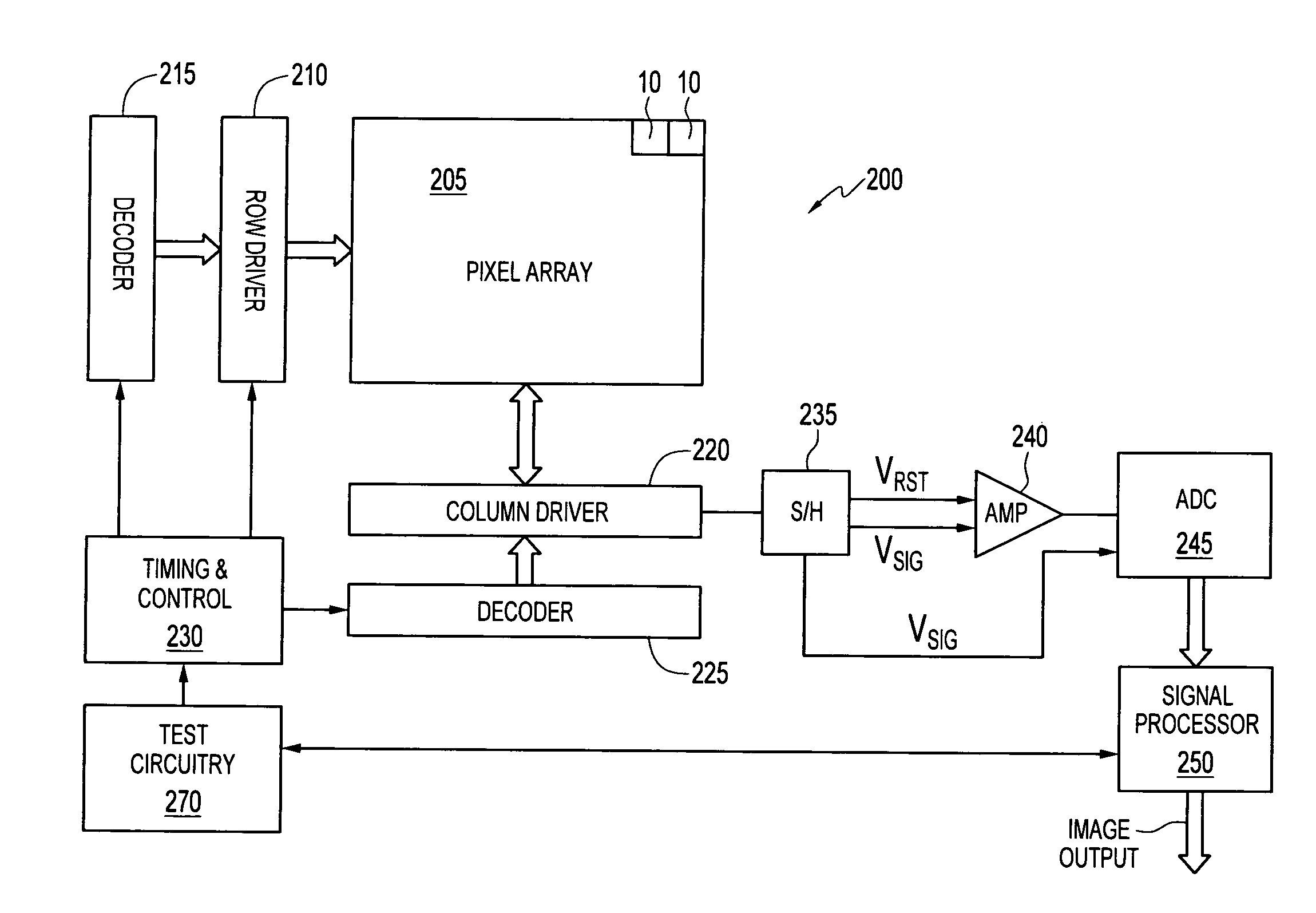
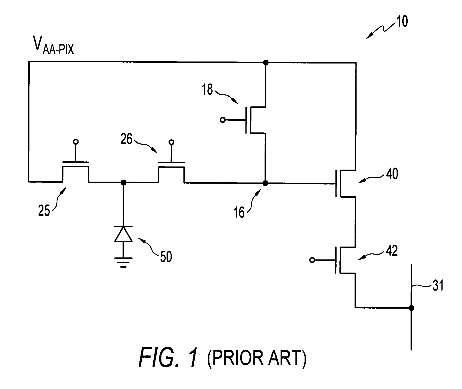
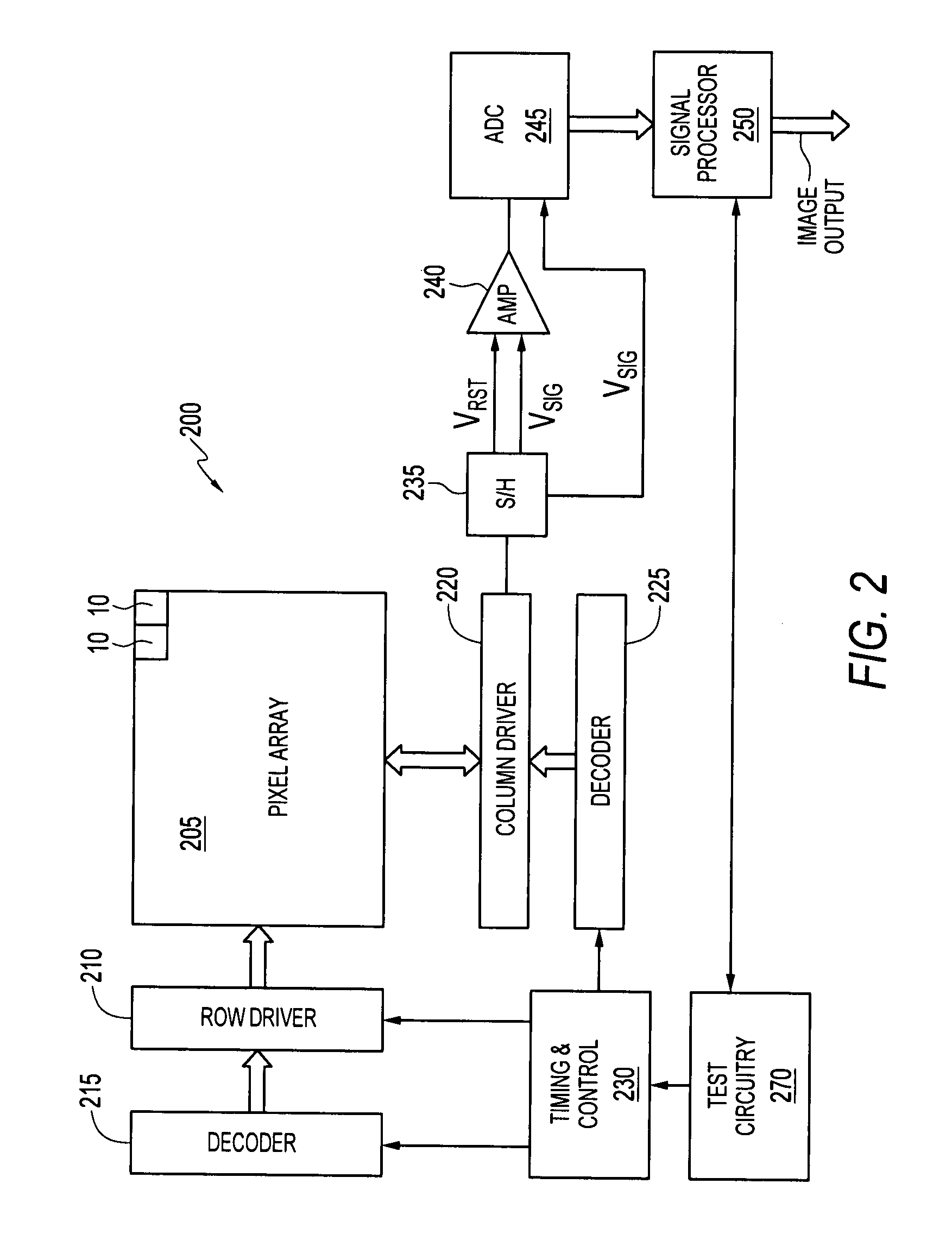
[0013]FIG. 2 shows a CMOS imaging device 200. The imaging device 200 includes a pixel array 205 having a plurality of pixels 10 (FIG. 1) arranged in columns and rows. It should be noted that although pixel 10 is shown as a 5-transistor (5T) configuration with an antiblooming transistor 26, other pixel configurations may be employed in imaging device 200. For example, pixels can include a shutter transistor coupled between the photoconversion device 50 and the transfer transistor 26 to have a 6-transistor (6T) configuratio...
PUM
 Abstract
Description
Claims
Application Information