Switching device with reduced intermodulation distortion

a switching device and intermodulation distortion technology, applied in the field of electrical circuits, can solve the problems of increasing the semiconductor die area consumed by the switching device, signal loss in the switching device, undesired increase in the cost of the switching device, etc., and achieve the effect of reducing the intermodulation distortion

Active Publication Date: 2010-10-19
SKYWORKS SOLUTIONS INC
View PDF40 Cites 47 Cited by
  • Summary
  • Abstract
  • Description
  • Claims
  • Application Information

AI Technical Summary

Problems solved by technology

However, increasing the number of FETs in each switching arm undesirably increases the semiconductor die area consumed by the switching device and signal loss in the switching device.
However, this approach can undesirably increase the cost of the switching device.

Method used


Image

  • Switching device with reduced intermodulation distortion
  • Switching device with reduced intermodulation distortion
  • Switching device with reduced intermodulation distortion

Examples


Embodiment Construction

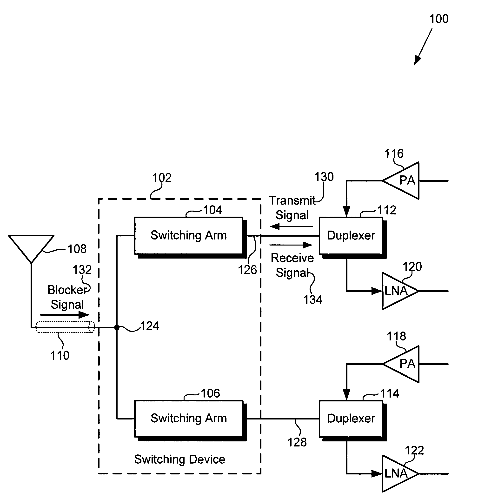
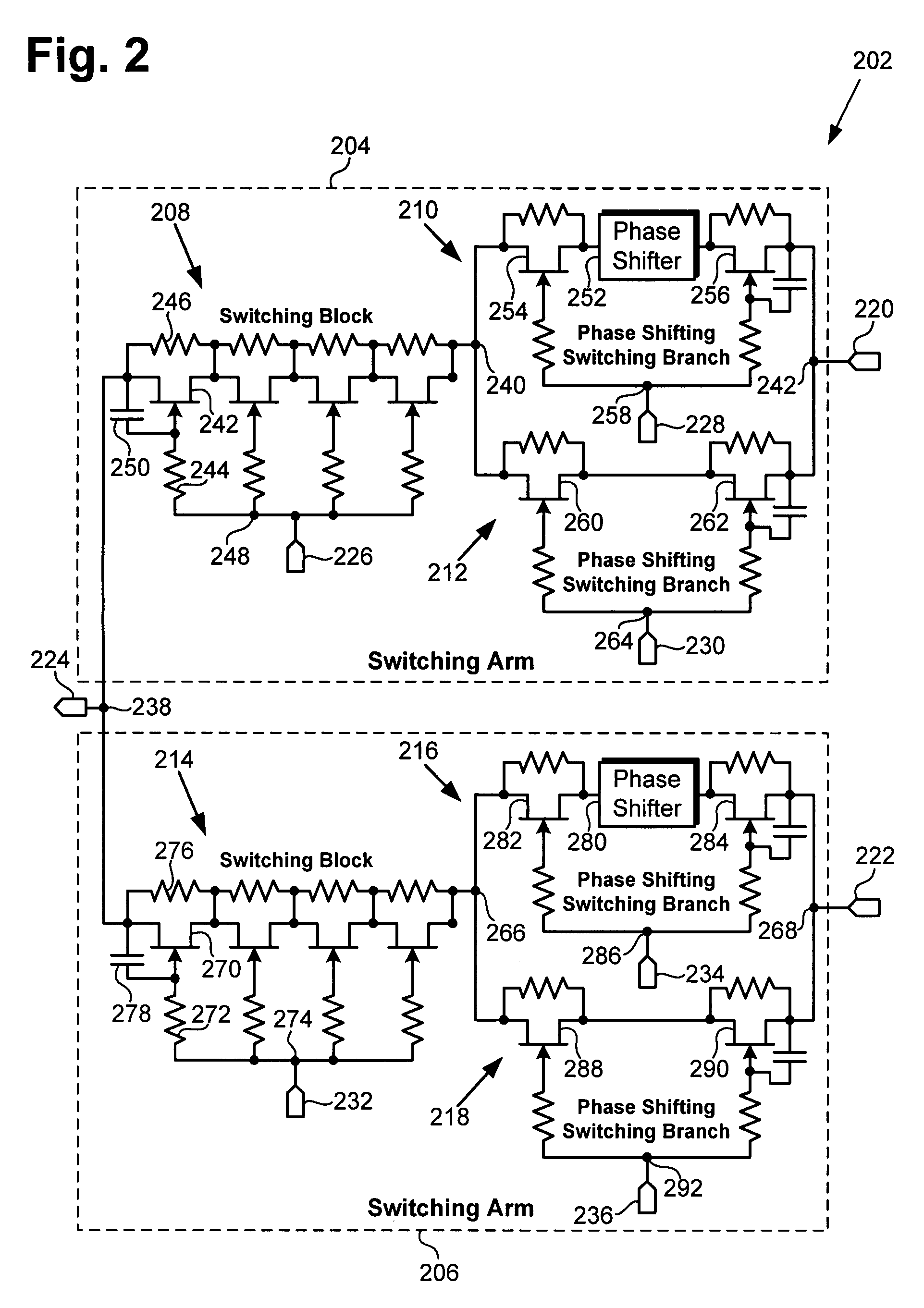
[0014]The present invention is directed to a switching device with reduced intermodulation distortion. The following description contains specific information pertaining to the implementation of the present invention. One skilled in the art will recognize that the present invention may be implemented in a manner different from that specifically discussed in the present application. Moreover, some of the specific details of the invention are not discussed in order not to obscure the invention. The specific details not described in the present application are within the knowledge of a person of ordinary skill in the art.

[0015]The drawings in the present application and their accompanying detailed description are directed to merely exemplary embodiments of the invention. To maintain brevity, other embodiments of the invention which use the principles of the present invention are not specifically described in the present application and are not specifically illustrated by the present dr...


PUM


Abstract

According to one exemplary embodiment, a switching device with phase selection terminals to select between at least two phase shifting modes to reduce intermodulation distortion in the switching device includes a first phase selection terminal to select a first phase shifting mode of the switching device by enabling a first phase shifter in a first phase shifting switching branch coupled to an input of the switching device. The switching device further includes a second phase selection terminal to select a second phase shifting mode of the switching device by enabling a second phase shifting switching branch coupled to the switching device input. The intermodulation distortion in the switching device is reduced by selecting one of the first and second phase shifting modes. The switching device may further include a number of FETs coupled in series between an output of the switching device and the first and second phase shifting switching branches.

Description

BACKGROUND OF THE INVENTION[0001]1. Field of the Invention[0002]The present invention is generally in the field of electrical circuits. More specifically, the invention is in the field of high-frequency switching circuits.[0003]2. Related Art[0004]High-frequency switching devices, such as high-frequency switching devices having multiple inputs and a shared output, can be used in mobile communication devices, such as cellular handsets, to provide operation at more than one frequency. For example, a high-frequency switching device can be used in a cellular handset operating in a system using a Global System for Mobile Communications (GSM) communications standard to enable the cellular handset to operate either at a low band frequency of 900.0 MHz or a high band frequency of 1800.0 MHz by selectively coupling a corresponding input to the shared output. For high-frequency switching devices, such as high-frequency switching devices used in mobile communication devices, there is a continu...

Claims


Application Information

Patent Timeline
Patent Type & Authority Patents(United States)
IPC IPC(8): H04B1/44
CPCH01P1/15
Inventor PRIKHODKO, DIMANABOKIN, SERGEYKLIMASHOV, OLEKSEYSPRINKLE, STEVEN C.TKACHENKO, GENE A.CARTER, RICHARD A.
Owner SKYWORKS SOLUTIONS INC
Why Eureka
Try Eureka