Shift register

a technology of shift register and shift register, applied in the field of shift register, can solve the problems of uneven display of/b> and discrepancy of threshold voltag

Active Publication Date: 2011-03-15
AU OPTRONICS CORP
View PDF5 Cites 13 Cited by
  • Summary
  • Abstract
  • Description
  • Claims
  • Application Information

AI Technical Summary

Benefits of technology

[0008]It is therefore an object of the present invention to provide a shift register capable of compensating a threshold voltage variation of a transistor, thereby effectively solving the above-mentioned problem existing in the prior art.

Problems solved by technology

Unfortunately, regarding the gate driver 14 manufactured with an amorphous silicon (a-Si) technology, the liquid crystal display 12 may display unevenly due to a voltage stress phenomenon which causes a discrepancy of threshold voltages of any two transistors.

Method used


Image

  • Shift register
  • Shift register
  • Shift register

Examples


first embodiment

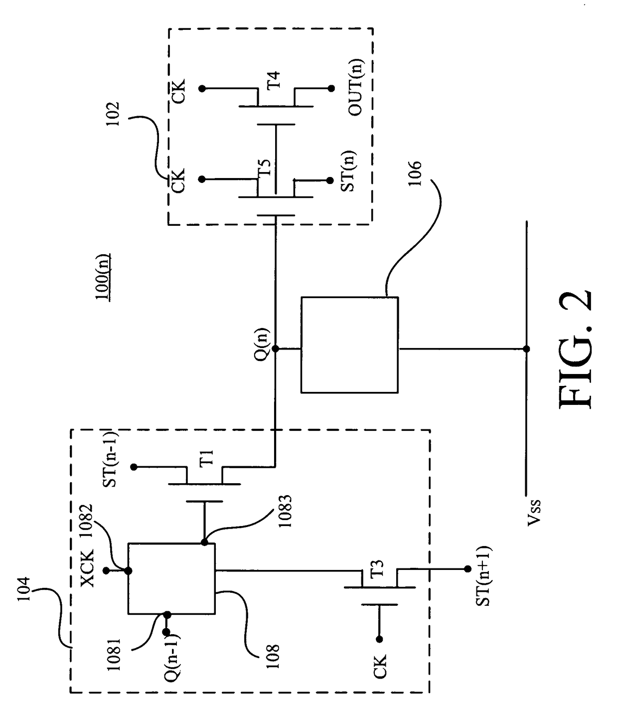
[0025]Referring to FIG. 3A illustrating a circuit diagram of a stage of the shift register according to the present invention, the pull-up driving circuit 104 is coupled to the pull-up circuit 102 at the input node Q(n). In this embodiment, the control circuit 108 comprises a second transistor T2 of which a gate is coupled to the input node Q(n−1) of the stage 100 (n−1), and a drain is coupled to the second clock signal XCK. The first transistor T1 comprises a gate coupled to a source of the second transistor T2, a drain coupled to the driving signal end ST(n−1) of the stage 100 (n−1), and a source coupled to the input node Q(n). The third transistor T3 comprises a gate coupled to the clock signal CK, a drain coupled to the source of the second transistor T2, and a source of a driving signal end of the next stage 100 (n+1).

[0026]The pull-up circuit 102 comprises a fourth transistor T4 and a fifth transistor T5. The fourth transistor T4 comprises a drain coupled to the first clock si...

third embodiment

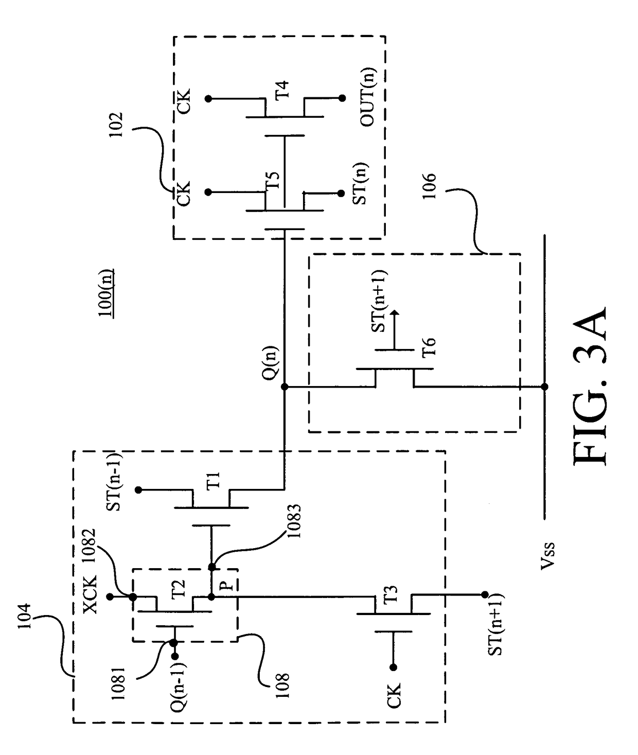
[0031]Referring to FIG. 5A illustrating a circuit diagram of a stage 300 (n) of the shift register according to the present invention, the pull-up circuit 204 shown in FIG. 5A is identical to the pull-up circuit 104 shown in FIG. 3A except a lack of the transistor T3. In this embodiment, the voltage level at the node P still to be pulled down to the low voltage VL via the transistor T1, in order to reduce the leakage current of the transistor T2. In addition, the gate and the source of the transistor T2 may be coupled to the input node Q(n−1) of the stage 300 (n−1) and the second clock XCK, respectively.

fourth embodiment

[0032]Referring to FIG. 5B illustrating a circuit diagram of a stage 400 (n) of the shift register according to the present invention, the gate of the transistor T2 may be coupled to the input node Q(n−1) of the stage 400 (n−1) or supply voltage VDD. The drain of the transistor T2 may be coupled to the second clock signal XCK or the driving signal end ST(n−1) of the stage 400 (n−1).

[0033]The shift register of the present embodiment can be applied to the gate driver of a LCD.

[0034]Compared to prior art, the present inventive shift register comprises the first transistor T1 and the third transistor T3, so that the voltage level on the gate of the first transistor T1 is controlled by means of the transistor T3 to compensate a threshold voltage variation of a transistor T1.


PUM


Abstract

A shift register includes a plurality of stages cascade-connected with each other. Each stage includes a pull-up circuit, a pull-up driving circuit, and a pull-down circuit. The pull-up circuit coupled to a first clock signal is used for providing an output signal. The pull-up driving circuit includes a control circuit and a first transistor. The control circuit has a gate coupled to a previous stage, and a drain coupled to a second clock signal. The first transistor includes a gate coupled to the source of the control circuit, a drain coupled to a driving end of the previous stage, and a source coupled to a first input end. The pull-down circuit pulls down voltage on the first input end.

Description

BACKGROUND OF THE INVENTION[0001]1. Field of the Invention[0002]The present invention relates to a shift register, and more particularly, to a shift register capable of compensating a threshold voltage variation of a transistor.[0003]2. Description of the Related Art[0004]With a rapid development of monitor types, novel and colorful monitors with high resolution, e.g., liquid crystal displays (LCDs), are indispensable components used in various electronic products such as monitors for notebook computers, personal digital assistants (PDAs), digital cameras, and projectors. The demand for the novelty and colorful monitors has increased tremendously.[0005]Referring to FIG. 1 showing a functional block diagram of a conventional liquid crystal display 10, the liquid crystal display 10 includes a liquid crystal panel 12, a gate driver 14, and a source driver 16. The liquid crystal panel 12 includes a plurality of pixels, each pixel having three pixel units 20 indicating three primary colo...

Claims


Application Information

Patent Timeline
Patent Type & Authority Patents(United States)
IPC IPC(8): G11C19/00
CPCG11C19/28G09G2310/0286G09G2320/0266
Inventor CHEN, WEN-PINCHANG, LEE-HSUNHSU, JE-HAO
Owner AU OPTRONICS CORP
Why Eureka
Try Eureka