Circuit for calibrating impedance and semiconductor apparatus using the same

a technology for semiconductor apparatus and circuits, applied in logic circuit coupling/interface arrangements, pulse techniques, instruments, etc., can solve the problems of reducing the layout margin available for semiconductor apparatus, adversely affecting the calibration operation of impedance, etc., and achieve the effect of improving the layout margin

Active Publication Date: 2011-08-02
SK HYNIX INC
View PDF17 Cites 38 Cited by
  • Summary
  • Abstract
  • Description
  • Claims
  • Application Information

AI Technical Summary

Benefits of technology

[0014]Embodiments of the present invention include a circuit for calibrating impedance and a semiconductor apparatus using the same so as to improve layout margin.

Problems solved by technology

Process / voltage / temperature (PVT) variation of the die can adversely affect the impedance calibration operation.
However, a drawback of the semiconductor apparatus configured with external resistance is the increased circuit area occupied by the resistance device and the additional component, such as a line, for connecting the external resistance to its corresponding die, thereby reducing the layout margin available for the semiconductor apparatus.

Method used


Image

  • Circuit for calibrating impedance and semiconductor apparatus using the same
  • Circuit for calibrating impedance and semiconductor apparatus using the same
  • Circuit for calibrating impedance and semiconductor apparatus using the same

Examples


Embodiment Construction

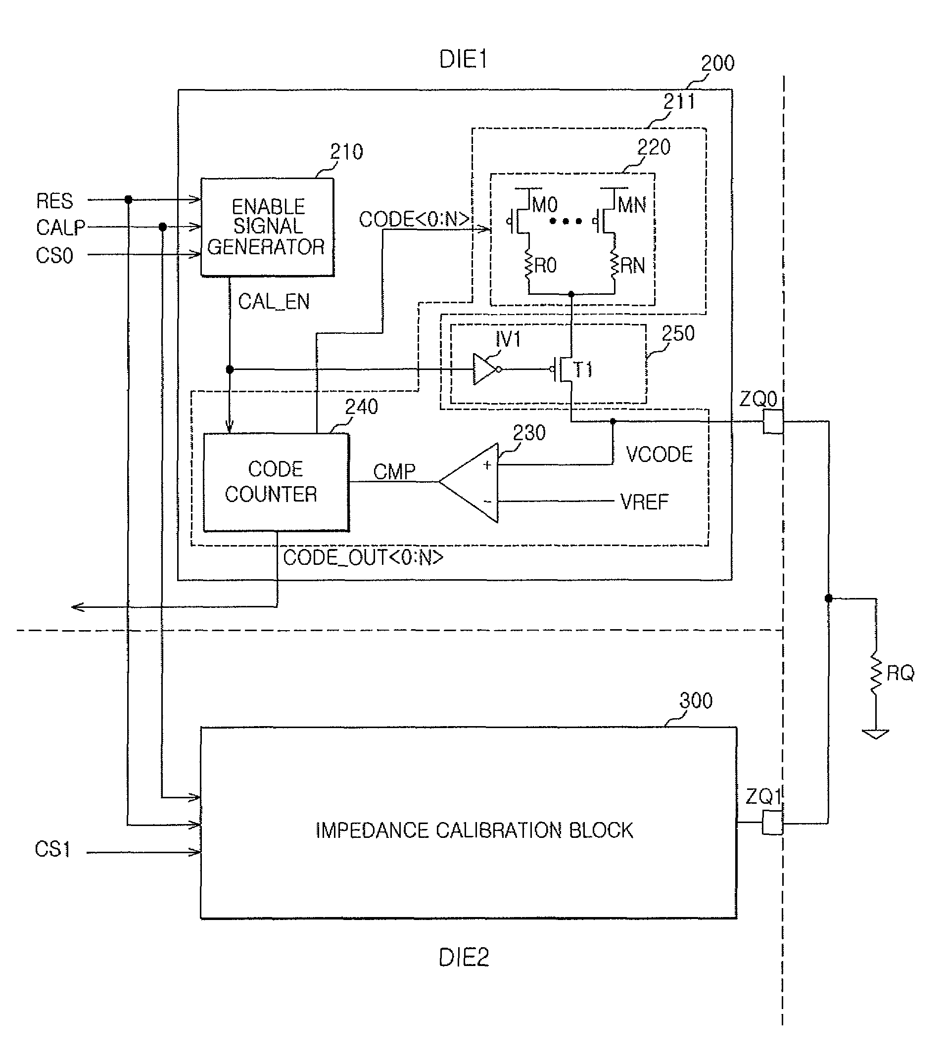
[0027]Hereinafter, preferred embodiments of the present invention will be described in more detail with reference to the accompanying drawings.

[0028]In an embodiment of the present invention different dies share one external resistance for performing an impedance calibration operation. The dies are controlled to perform the impedance calibration operation at different timings by using signals for selecting the dies.

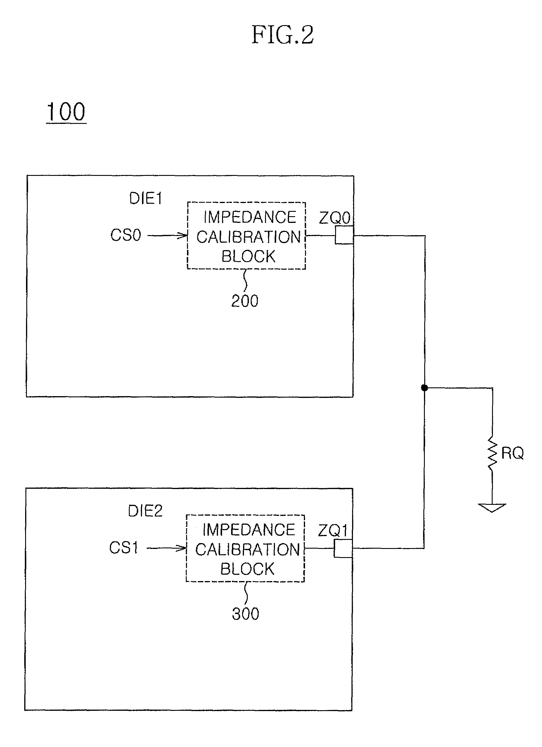
[0029]FIG. 2 is a block diagram of an exemplary semiconductor apparatus 100 according to one embodiment of the present invention.

[0030]In the embodiment shown in FIG. 2, the semiconductor apparatus 100 is configured to include two dies DIE1 and DIE2.

[0031]In an embodiment, the two dies DIE1 and DIE2 are configured to include impedance calibration blocks 200 and 300, respectively.

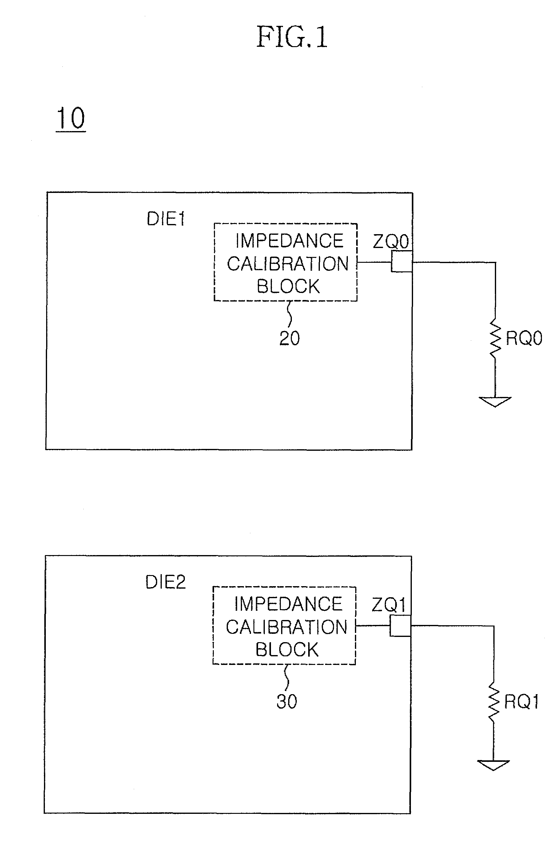
[0032]As shown in FIG. 2, the impedance calibration blocks 200 and 300 are commonly coupled to the same external resistance RQ through external resistance connection electrodes ZQ0 and ZQ1.

[0033]D...


PUM


Abstract

A circuit for calibrating impedance includes an enable signal generator, a code generator and a connection controller. The enable signal generator generates an enable signal in response to a chip selection signal. The code generator generates an impedance calibration code in response to the enable signal by using an external resistance coupled to an electrode. The connection controller controls connection between the code generator and the electrode in response to the enable signal.

Description

CROSS-REFERENCES TO RELATED PATENT APPLICATION[0001]The present application claims priority under 35 U.S.C 119(a) to Korean Application No. 10-2009-0058932, filed on Jun. 30, 2009, in the Korean Intellectual Property Office, which is incorporated herein by reference in its entirety as set forth in full.BACKGROUND[0002]1. Technical Field[0003]Embodiments of the present invention relate generally to semiconductor circuit technology, and more particularly, to a circuit for calibrating impedance and a semiconductor apparatus using the same.[0004]2. Related Art[0005]Semiconductor packaging is a technology used for the purpose of improving the efficiency of integration. A multi-chip package type in which two or more dies (alternatively, referred to as “chip”) are packaged is prevalent in semiconductor packaging technology.[0006]Each of the dies of the multi-chip package is an independent component. In a case in which each die is a memory device, such as dynamic random access memory (DRAM)...

Claims


Application Information

Patent Timeline
Patent Type & Authority Patents(United States)
IPC IPC(8): H03K17/16
CPCG11C5/06H01L2224/16H01L25/0657G11C7/10
Inventor PARK, NAK KYU
Owner SK HYNIX INC
Why Eureka
Try Eureka