
Refresh control circuit of semiconductor apparatus

a control circuit and semiconductor technology, applied in the field of semiconductor apparatus, can solve problems such as significant increase in circuit area, and achieve the effect of improving the layout margin of semiconductor apparatus

Active Publication Date: 2015-07-28
SK HYNIX INC
View PDF7 Cites 0 Cited by
  • Summary
  • Abstract
  • Description
  • Claims
  • Application Information

AI Technical Summary

Benefits of technology

The refreshing control circuit of this patent aims to make the circuit more efficient in terms of space usage, which will enable better placement of components in the semiconductor device. The main technical effect of this invention is to minimize the area of the delay circuit in the refresh control circuit.

Problems solved by technology

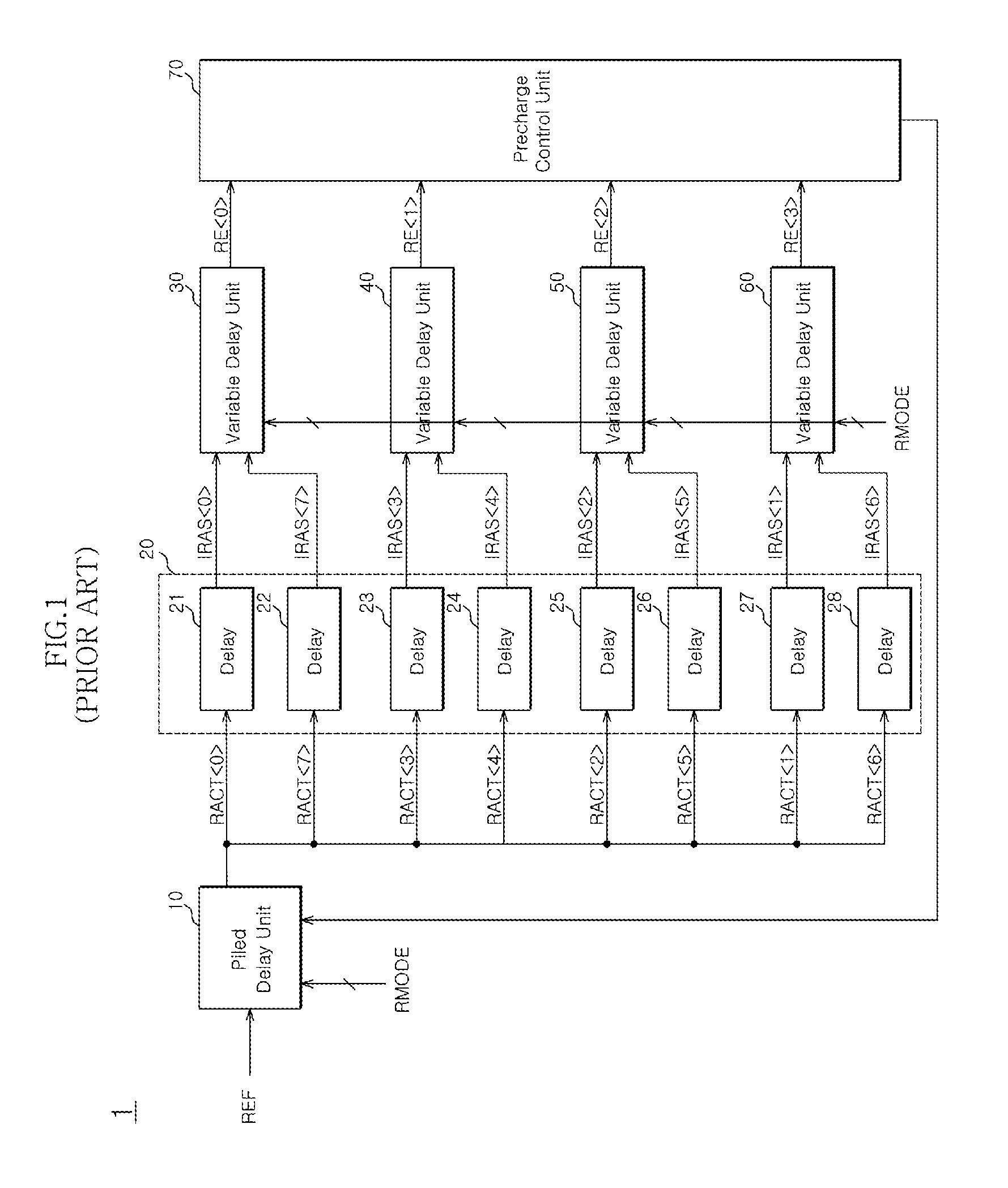
Accordingly, when supporting a piled operation beyond the 4 piled operation such as an 8 piled operation, eight variable delay units are required, resulting in a significant increase in circuit area.

Method used


Image

  • Refresh control circuit of semiconductor apparatus
  • Refresh control circuit of semiconductor apparatus
  • Refresh control circuit of semiconductor apparatus

Examples


Embodiment Construction

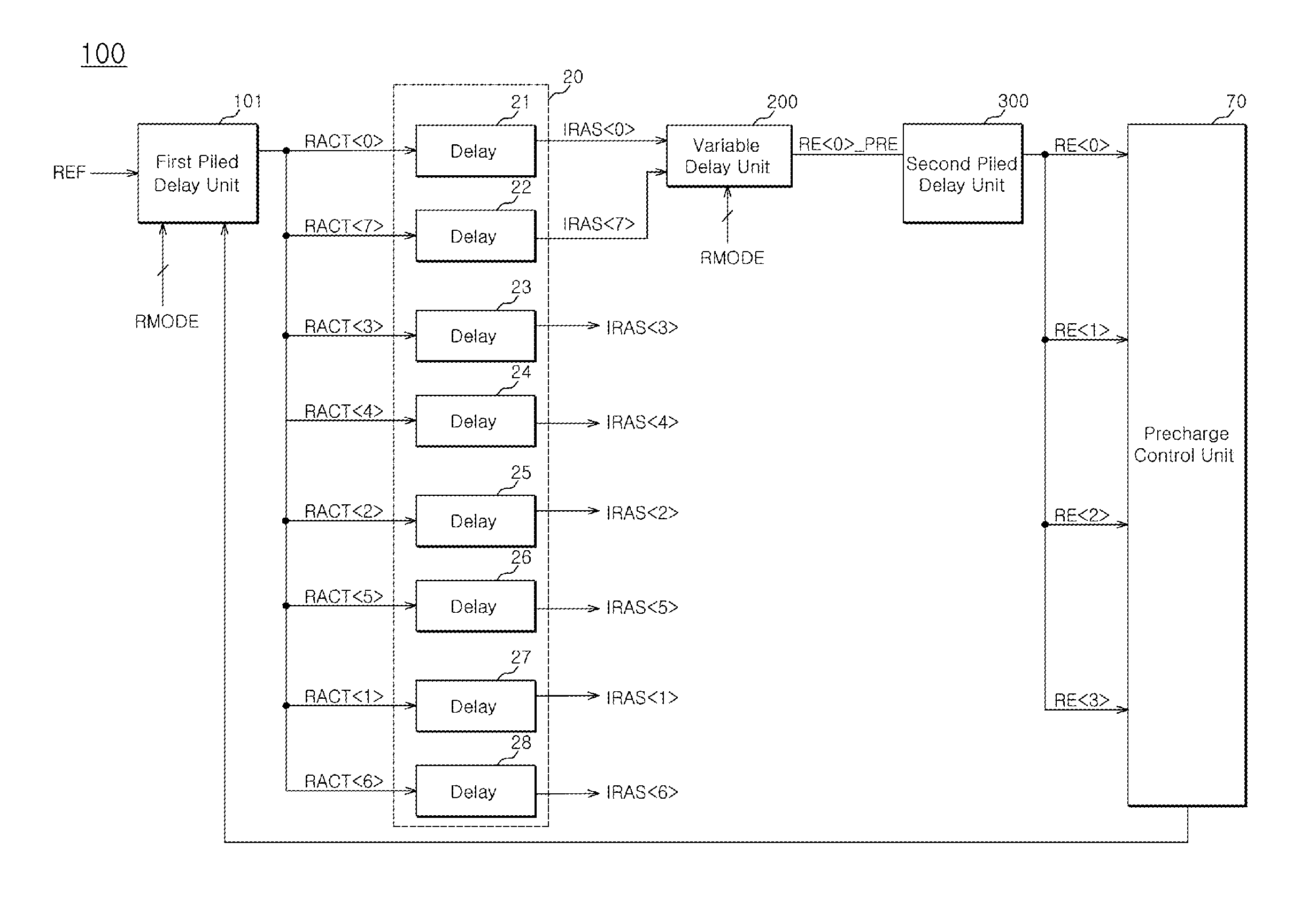
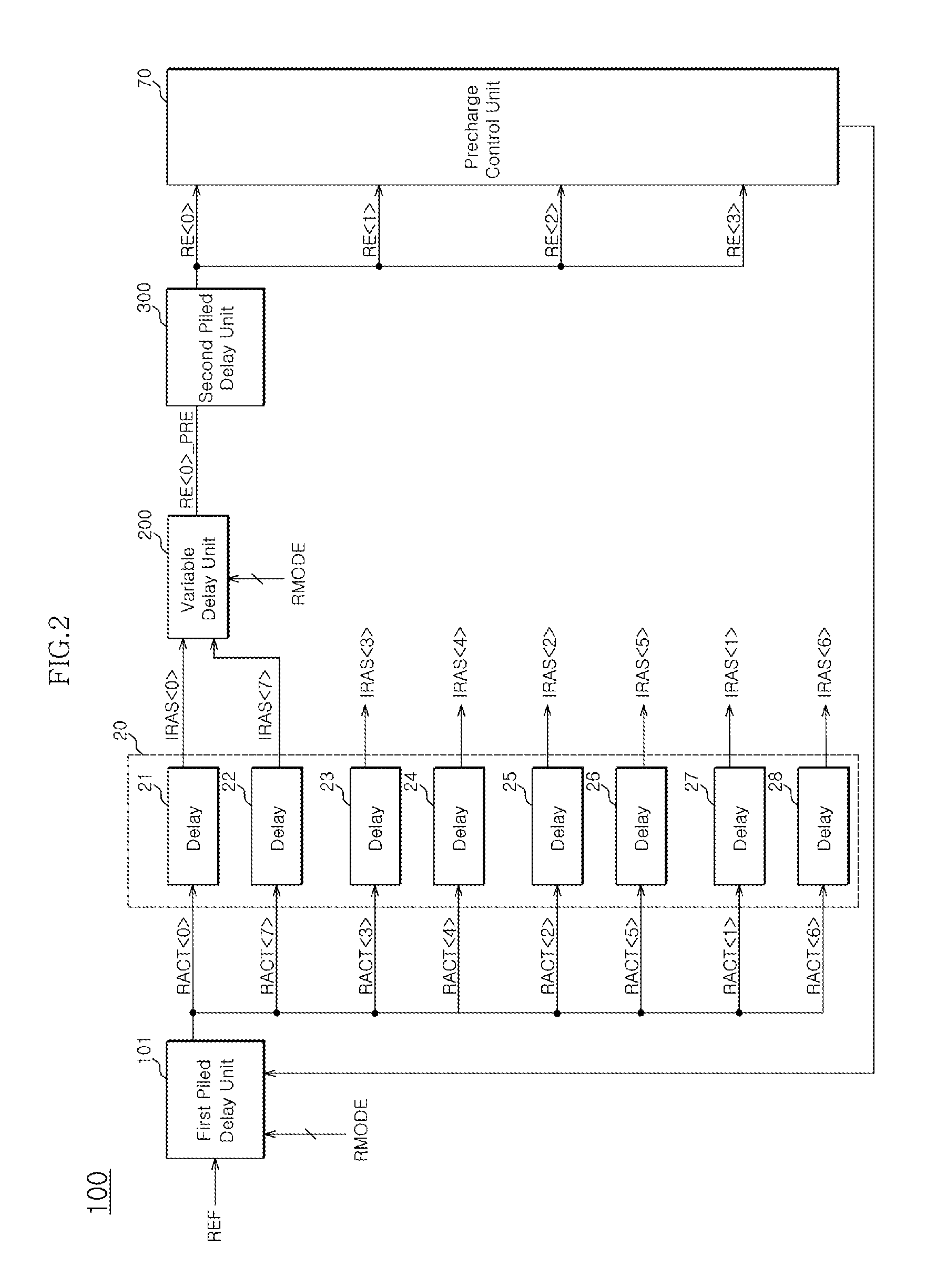
[0028]Hereinafter, a refresh control circuit of a semiconductor apparatus according to the present invention will be described in detail with reference to the accompanying drawings through various embodiments.

[0029]A semiconductor apparatus includes a memory area for storing data.

[0030]A memory bank BK may be used as a unit for dividing the memory area.

[0031]Embodiments of the present invention corresponds to a refresh control circuit 100 when a semiconductor apparatus includes first to eight memory banks BK0 to BK7 (not illustrated) as an example for convenience of description. However, the present invention is not limited to eight memory banks.

[0032]FIG. 2 is a block diagram of a refresh control circuit 100 of a semiconductor apparatus according to an embodiment of the present invention.

[0033]As illustrated in FIG. 2, the refresh control circuit 100 includes a first piled delay unit 101, a delay unit 20, a variable delay unit 200, a second piled delay unit 300, and a precharge con...


PUM


Abstract

A refresh control circuit of a semiconductor apparatus includes a variable delay unit configured to delay a signal that is activated quickest among a plurality of row address strobe signals activated at a predetermined time interval by a predetermined time, and to generate a preliminary pulse signal, and a piled delay unit configured to delay the preliminary pulse signal by various times, and to generate a plurality of refresh period pulse signals that are sequentially activated.

Description

CROSS-REFERENCES TO RELATED APPLICATION[0001]The present application claims priority under 35 U.S.C. §119(a) to Korean application number 10-2012-0125570, filed on Nov. 7, 2012, in the Korean Intellectual Property Office, which is incorporated herein by reference in its entirety.BACKGROUND[0002]1. Technical Field[0003]The present invention relates generally to a semiconductor apparatus, and more particularly, to a refresh control circuit of a semiconductor apparatus.[0004]2. Related Art[0005]As illustrated in FIG. 1, a refresh control circuit 1 of a semiconductor apparatus according to the conventional art includes a piled delay unit 10, a delay unit 20, first to fourth variable delay units 30, 40, 50, and 60, and a precharge control unit 70.[0006]The piled delay unit 10 generates a plurality of row active signals RACT<0:7> in response to a refresh signal REF and a refresh mode signal RMODE.[0007]The plurality of row active signals RACT<0:7> may then be activated at a pr...

Claims


Application Information

Patent Timeline
Patent Type & Authority Patents(United States)
IPC IPC(8): G11C7/00G11C11/406G11C11/4094G11C7/22
CPCG11C11/40611G11C11/4094G11C11/40618G11C7/222G11C2211/4065G11C7/22G11C11/406
Inventor IM, JONG MAN
Owner SK HYNIX INC
Learn More