Via structure with dual current path

a current path and structure technology, applied in the field ofvia structure, can solve the problems of corresponding increase in inductance and, hence, electronic emissions, interference with other signals in the system, increased emissions and noise cross-talk,

Inactive Publication Date: 2002-11-12
IBM CORP
View PDF5 Cites 81 Cited by
  • Summary
  • Abstract
  • Description
  • Claims
  • Application Information

AI Technical Summary

Problems solved by technology

Increasing the loop area results in a corresponding increase in inductance and, hence, electronic emissions, i.e., noise.
Such

Method used


Image

  • Via structure with dual current path
  • Via structure with dual current path
  • Via structure with dual current path

Examples


first embodiment

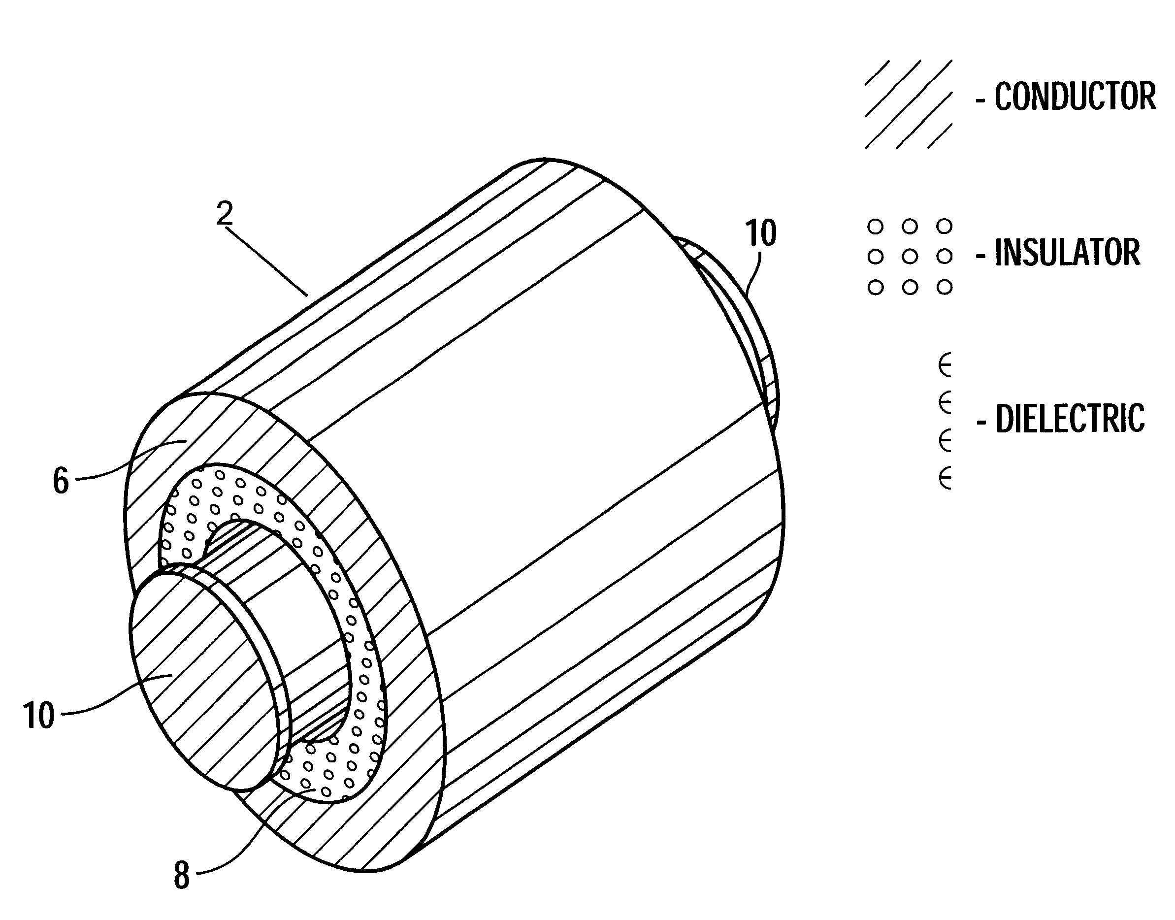
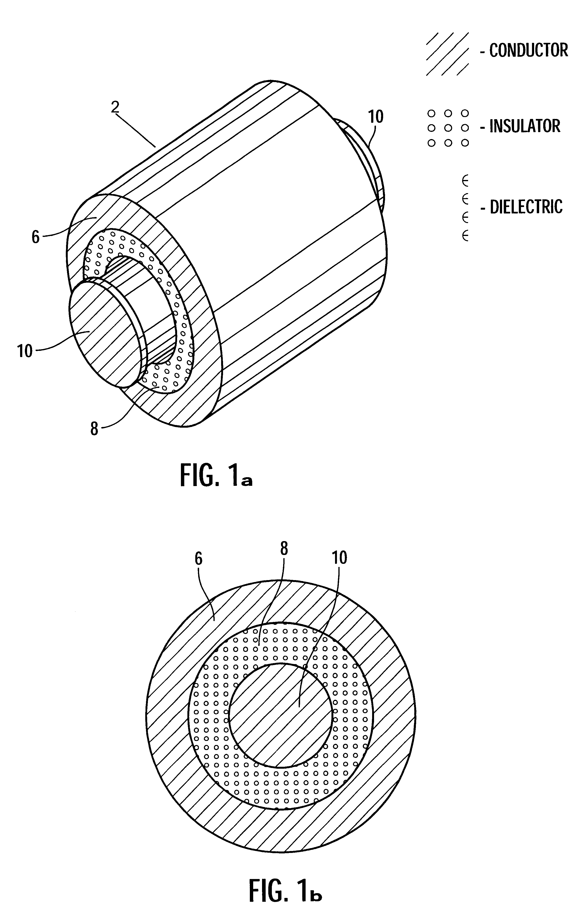
FIG. 1a illustrates a perspective view of a via structure in accordance with the present invention;

FIG. 1b illustrates a cross-sectional view perpendicular to the axis of the via structure shown in FIG. 1a;

second embodiment

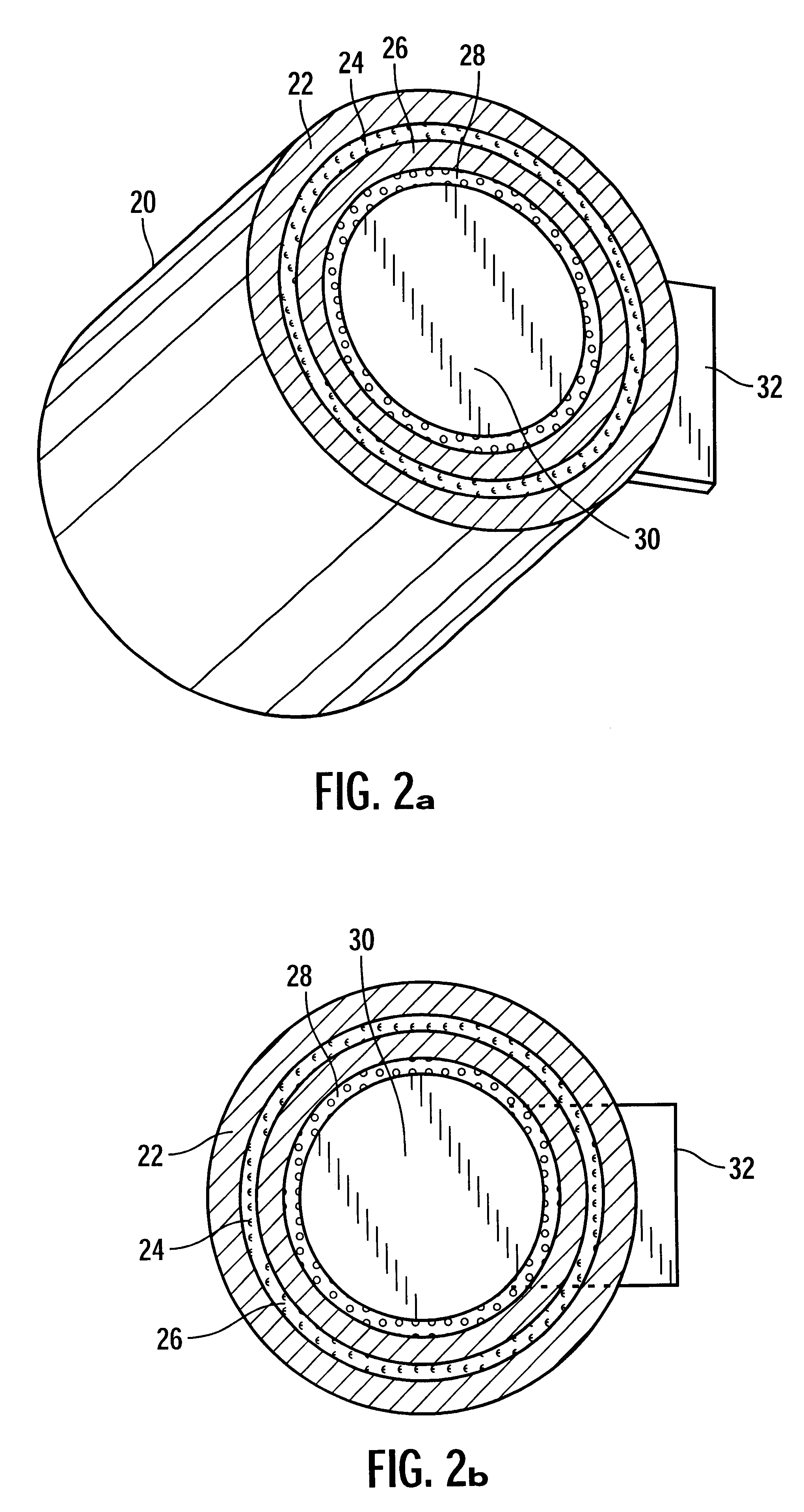
FIG. 2a illustrates a perspective view of a via structure in accordance with the present invention;

FIG. 2b illustrates a cross-sectional view perpendicular to the axis of the via structure shown in FIG. 2a;

FIG. 3 illustrates a perspective view of the via structure of FIGS. 1a, b disposed through layers;

FIG. 4 illustrates a cross-sectional view along the axis of the via structure shown in FIG. 1a; and

FIGS. 5-9 illustrate cross-sectional views along the axis of alternative embodiments of the via structure.

In the following description, reference is made to the accompanying drawings which form a part thereof and which illustrate several embodiments of the present invention. In the drawings, depicted elements are not necessarily drawn to scale and like or similar elements may be designated by the same reference numeral throughout the several views. Further, it is understood that other embodiments may be utilized and structural and operational changes may be made without departing from th...


PUM


Abstract

Provided is a via for use in a printed circuit board or integrated circuit having first, second, third, and fourth layers. The via includes a first path capable of transmitting a forward current from the first to the second layer and a second path capable of transmitting a return current resulting from the forward current from the third to the fourth layer to return to a source of the forward current.

Description

1. Field of the InventionThe present invention relates to a via structure that reduce inductance in the current path when used in printed circuit boards and integrated circuits.2. Description of the Related ArtA printed circuit board comprises a thin plate formed of multiple layers onto which chips and other electronic components, such as integrated circuits, are mounted. Computers consist of one or more boards, often called cards or adapters. Each layer of the printed circuit board includes metal paths ending in contact pads. An electronic device would transfer signals to a network of metal paths through the contact pad to communicate over the metal paths with other electronic devices on the same or different layers of the substrate. A via structure extends through holes in the layers and interfaces with contact pads on different layers to allow signals to travel between layers through the via. In this way, the via provides a conductive path to communicate between conductive layers...

Claims


Application Information

Patent Timeline
IPC IPC(8): H05K1/16H05K1/11H05K1/02H05K3/42H01R12/51
CPCH05K1/0222H05K1/115H05K1/162H05K3/429H05K2201/09809
Inventor FRANA, ANDREW JAMESGILLILAND, DON ALAN
Owner IBM CORP
Why Eureka
Try Eureka