Apparatus and method for inspecting micro-structured devices on a semiconductor substrate

a semiconductor substrate and optical inspection technology, applied in the direction of measurement devices, instruments, material analysis, etc., can solve the problems of general inability or inability to meet the requirements of micro-structured samples inspection, and achieve the effect of automization of the overall system

Active Publication Date: 2012-04-10
VISTEC SEMICON SYST
View PDF11 Cites 22 Cited by
  • Summary
  • Abstract
  • Description
  • Claims
  • Application Information

AI Technical Summary

Benefits of technology

[0015]By using an autofocus system for focusing on the sample, wafer, mask or substrate with micro-structured components, the overall system can be automized, which is advantageous in particular with the in-line utilization in the production of wafers. With the aid of a PC, the images of the incident and transmitted-light system can be combined in such a way that they can be output together on an output apparatus, in particular a monitor.

Problems solved by technology

The prior art systems for inspecting wafers are almost exclusively designed for the incident-light inspection in the visual or UV ranges, and are generally not or not well suited for the inspection of micro-structured samples, such as encapsulated or embedded objects or wafers structured on both sides, and stacked structures of a plurality of wafers.

Method used


Image

  • Apparatus and method for inspecting micro-structured devices on a semiconductor substrate
  • Apparatus and method for inspecting micro-structured devices on a semiconductor substrate

Examples


Embodiment Construction

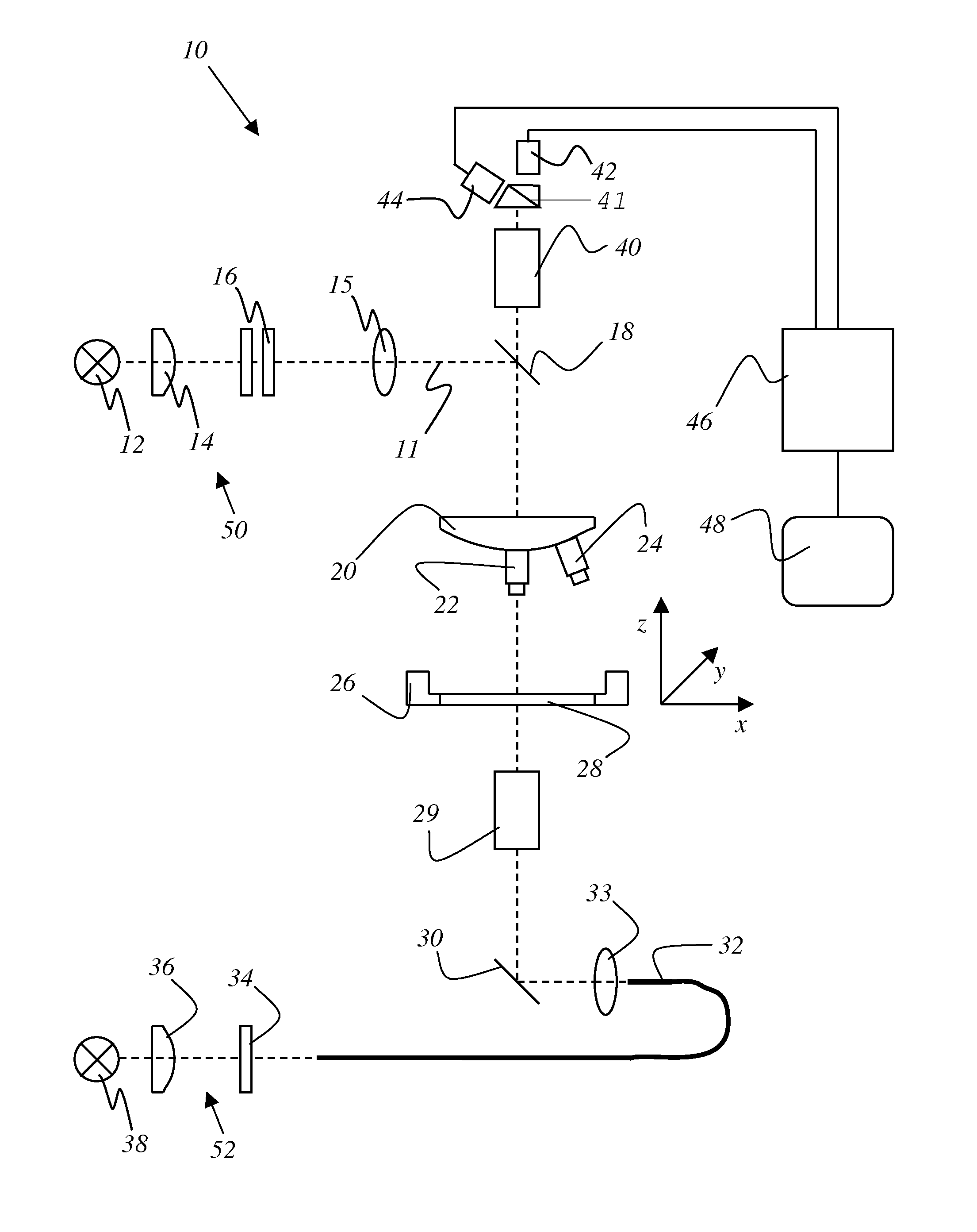
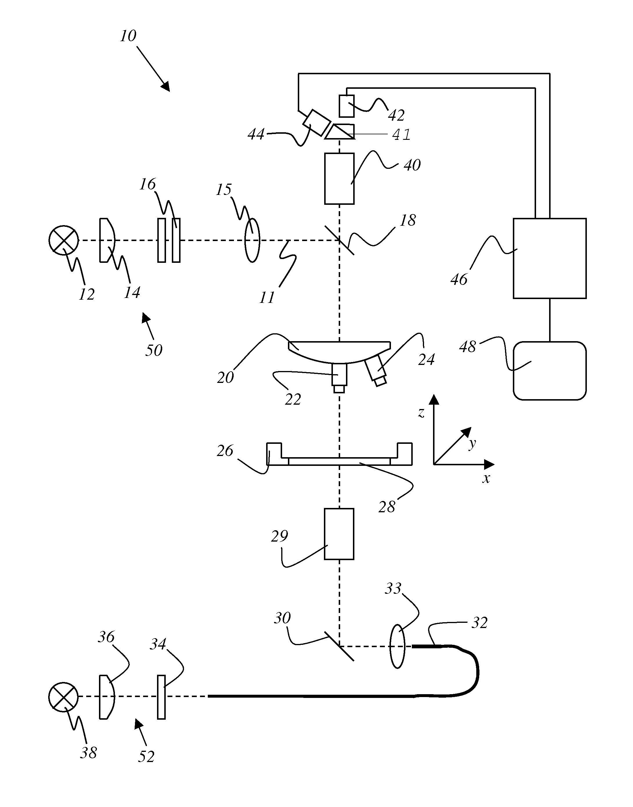
[0018]The single FIGURE schematically illustrates a characteristic structure according to the present invention, of a wafer inspection apparatus 10, in particular a microscope for observing a wafer 28. The term wafer inspection apparatus 10 should not be construed, however, as a limitation of the invention. With the aid of wafer inspection apparatus 10, micro-structured samples, such as wafers, masks or micro-structured devices (encapsulated or unencapsulated) on a substrate (usually a semiconductor substrate) can be inspected. The wafer inspection apparatus 10 has an incident-light illumination means 50. It essentially comprises an incident-light source 12 having its light directly or indirectly coupled onto wafer 28. For this purpose, the incident-light beam 11 can be passed through a collector 14. With the subsequent arrangement of one or more exchangeable filters 16, the light wavelength desired for illumination can be filtered from the optical spectral range. Furthermore, a swi...


PUM

PropertyMeasurementUnit
transparentaaaaaaaaaa
non-transparentaaaaaaaaaa
wavelength-aaaaaaaaaa

Abstract

Previously used examination devices and methods mostly operate with reflected visible or UV light to analyze microstructured samples of a wafer (38), for example. The aim of the invention is to increase the possible uses of said devices, i.e. particularly in order to represent structural details, e.g. of wafers that are structured on both sides, which are not visible in VIS or UV because coatings or intermediate materials are not transparent. Said aim is achieved by using IR light as reflected light while creating transillumination (52) which significantly improves contrast in the IR image, among other things, thus allowing the sample to be simultaneously represented in reflected or transmitted IR light and in reflected visible light.

Description

RELATED APPLICATIONS[0001]This application is a National Stage application of PCT application serial number PCT / EP2005 / 052351 filed on May 23, 2005 which in turn claims priority to German application serial number 10 2004 029 212.4 filed on Jun. 16, 2004.FIELD OF THE INVENTION[0002]The present invention relates to apparatus for the optical inspection of micro-structured samples, comprising a sample support on which the sample can be placed for inspection, and to a method of optically inspecting micro-structured samples, wherein a sample support is provided, on which the sample is placed for inspection, and an observation means, in particular a microscope, with which the sample is observed.BACKGROUND OF THE INVENTION[0003]For inspecting the surface of micro-structured samples, such as wafers, masks or micro-structured devices on a substrate, optical apparatus are particularly suitable. For example as known from EP 455 857 the inspection of the surface can be carried out by evaluating...

Claims


Application Information

Patent Timeline
Patent Type & Authority Patents(United States)
IPC IPC(8): G01N21/00G01N21/35G01N21/59G01N21/95G02B21/08
CPCG01N21/59G01N21/9501G02B21/088G01N21/9505
Inventor GRAF, UWEDANNER, LAMBERT
Owner VISTEC SEMICON SYST
Why Eureka
Try Eureka