Method of driving an image sensor with blooming current

a technology of image sensor and blooming current, which is applied in the field of driving image sensors, can solve the problems of limiting the dynamic range of linear image sensors, and increasing the size and cost of image sensors, so as to achieve the effect of minimizing the noise in the pixel of image sensors

Active Publication Date: 2013-11-26
SAMSUNG ELECTRONICS CO LTD
View PDF10 Cites 7 Cited by
  • Summary
  • Abstract
  • Description
  • Claims
  • Application Information

AI Technical Summary

Benefits of technology

[0015]Accordingly, an image sensor is driven for minimizing noise with conduction of blooming current.
[0028]In this manner, noise is minimized in the pixel of the image sensor from application of the noise-reducing voltage on the transfer gate during the first period of the integration mode. In addition, surplus electric charge is conducted away from the photo-detector from application of the blooming current voltage on the transfer gate during the second period of the integration mode.

Problems solved by technology

A dynamic range of the linear image sensor, however, may be limited to below about 75 dB.
However, size and cost of the image sensor are generally increased by such proposed methods since the charge storage capacity of a photo-detector (e.g., a photodiode) in a pixel should be increased resulting in a limit to the increase of the dynamic range.
Thus, the linear image sensor is not suitable for a device desired to have a small size.
The logarithmic image sensor, however, may have a long RC response time when the intensity of the received light is low.
Furthermore, the logarithmic image sensor is more sensitive to noise since the logarithmic image sensor outputs an electrical signal that is compressed with respect to the received light.
In that case, noise may be increased from dark current flowing below the transfer gate, especially at a high temperature.

Method used


Image

  • Method of driving an image sensor with blooming current
  • Method of driving an image sensor with blooming current
  • Method of driving an image sensor with blooming current

Examples


Embodiment Construction

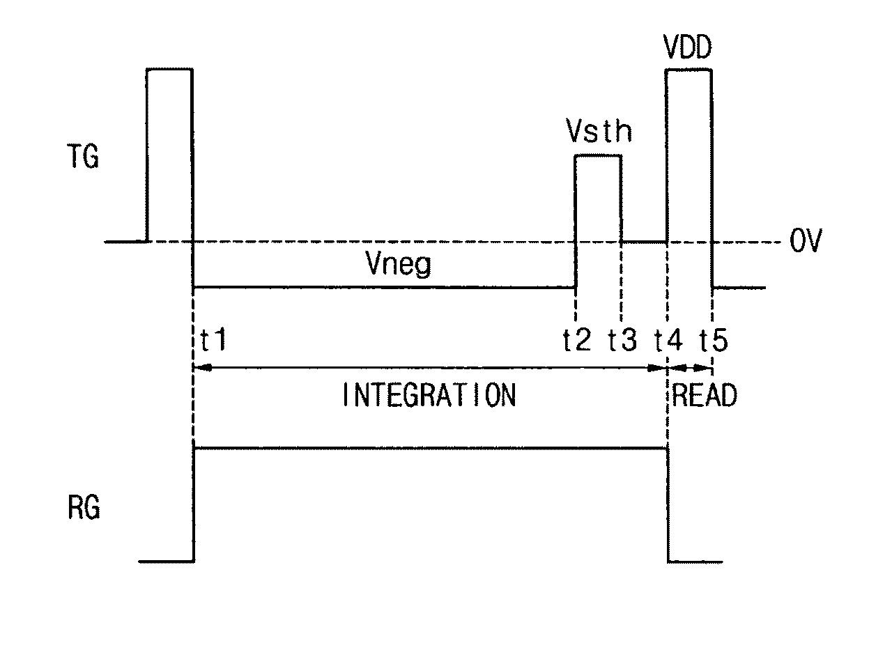
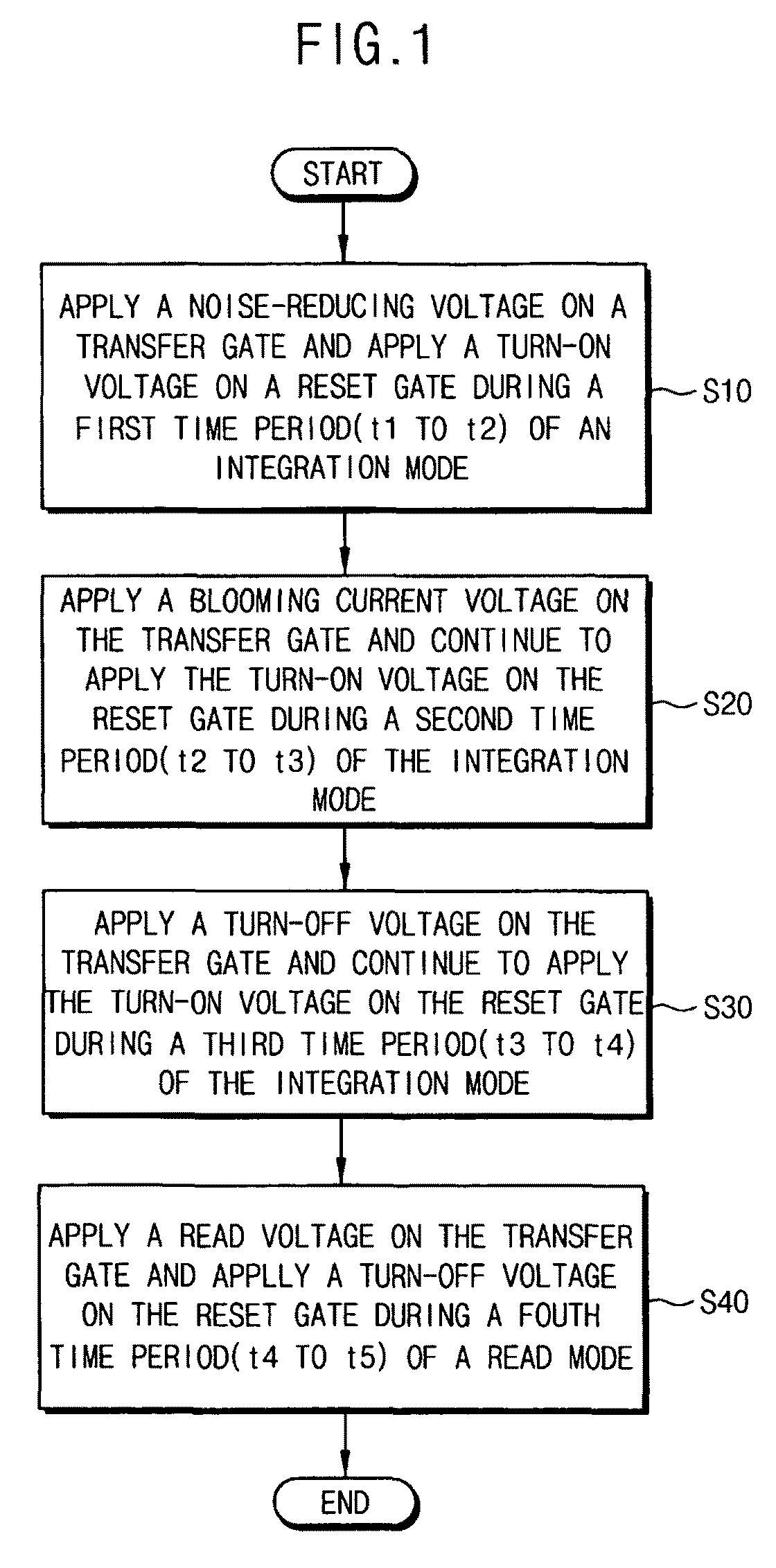
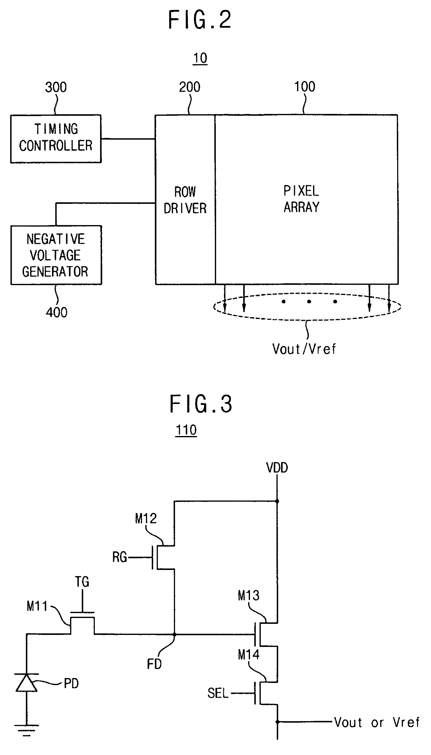
[0039]Example embodiments of the present invention are described herein with reference to the accompanying drawings. However, the present invention may be embodied in many different forms and should not be construed as limited to the example embodiments set forth herein. Rather, these example embodiments are described so that this disclosure is thorough and complete for fully conveying the scope of the present invention to those skilled in the art. In the drawings, the sizes and relative sizes of layers and regions may be exaggerated for clarity. Like numerals refer to like elements throughout.

[0040]It will be understood that, although the terms first, second, third etc. may be used herein to describe various elements, these elements should not be limited by these terms. These terms are used to distinguish one element from another. Thus, a first element discussed below could be termed a second element without departing from the teachings of the present invention. As used herein, the...


PUM


Abstract

For driving an image sensor having a pixel with a transfer gate formed between a photo-detector and a floating diffusion region, a noise-reducing voltage is applied on the transfer gate during a first period of an integration mode. A blooming current voltage is applied on the transfer gate during a second period of the integration mode. A read voltage is applied on the transfer gate during a read mode after the integration mode. The read voltage has a higher magnitude than the blooming current voltage. With application of the noise-reducing voltage, noise is reduced and a dynamic range is extended for the image sensor.

Description

[0001]This application claims priority under 35 USC §119 to Korean Patent Application No. 10-2007-117792, filed on Nov. 19, 2007 in the Korean Intellectual Property Office, the disclosure of which is incorporated herein in its entirety by reference.BACKGROUND[0002]1. Technical Field[0003]The present invention relates generally to image sensors, and more particularly, to a method of driving an image sensor for reduced noise and with blooming current flow.[0004]2. Description of the Related Art[0005]Image sensors convert optical images into electrical signals and are widely used in electronic devices, such as digital cameras, mobile phones, etc. The image sensors are generally divided into a charge-coupled device (CCD) image sensor and a complementary metal oxide semiconductor (CMOS) image sensor.[0006]The CCD image sensor consumes more power than the CMOS image sensor, but the CCD image sensor has less noise and better image quality in comparison with the CMOS image sensor. Since the...

Claims


Application Information

Patent Timeline
Patent Type & Authority Patents(United States)
IPC IPC(8): H04N5/335
CPCH04N5/3594H04N5/361H01L27/14656H04N25/583H04N25/623H04N25/63H04N25/57H04N25/60
Inventor LEE, JONG-JINKO, JU-HYUNAHN, JUNG-CHAK
Owner SAMSUNG ELECTRONICS CO LTD
Why Eureka
Try Eureka