High-resistance thin-film resistor and method of forming the resistor

a thin-film resistor, high-resistance technology, applied in the direction of resistor details, basic electric elements, solid-state devices, etc., can solve the problems of increasing the surface area of the thin-film resistor b, difficult or expensive use of exotic materials with high resistance, and increasing the resistance of thin-film resistors. , to achieve the effect of increasing the resistan

Active Publication Date: 2014-06-17
TEXAS INSTR INC
View PDF4 Cites 6 Cited by
  • Summary
  • Abstract
  • Description
  • Claims
  • Application Information

AI Technical Summary

Problems solved by technology

One of the drawbacks of thin-film resistor 140 is that it is difficult to increase the resistance of thin-film resistor 140.
Exotic materials that have high resistances, however, are often difficult or expensive to use in a conventional fabrication process.
Significantly increasing the length of thin-film resistor 140, however, significantly increases the surface area that thin-film resistor 140 consumes which, in turn, increases the size and cost of a die that includes thin-film resistor 140.

Method used


Image

  • High-resistance thin-film resistor and method of forming the resistor
  • High-resistance thin-film resistor and method of forming the resistor
  • High-resistance thin-film resistor and method of forming the resistor

Examples


Embodiment Construction

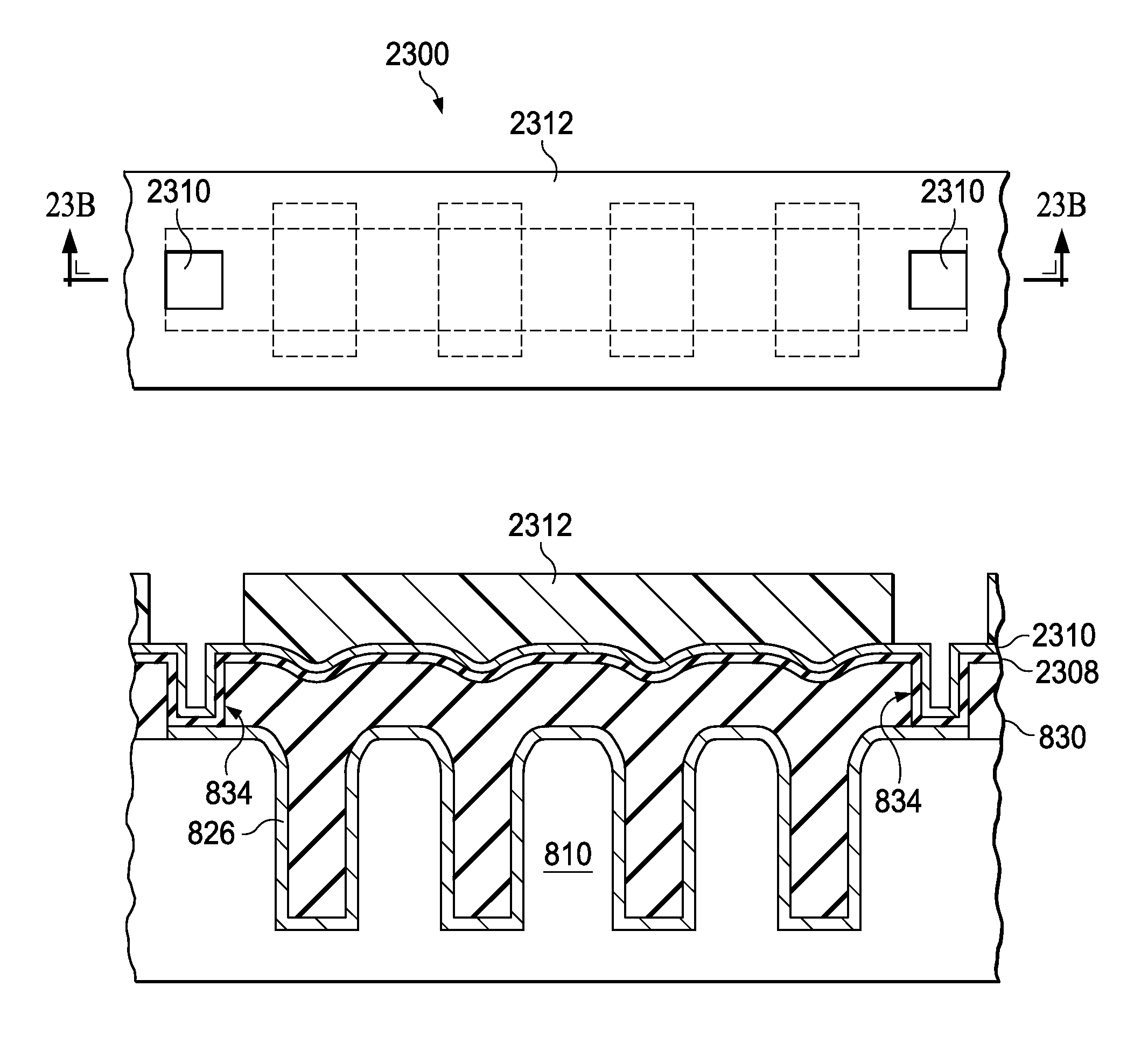
[0026]FIGS. 8A-8B to 13A-13B show a series of views that illustrate an example of a method 800 of forming a thin-film resistor in accordance with the present invention. FIGS. 8A-13A show a series of plan views, while FIGS. 8B-13B show a series of cross-sectional views taken along lines 8B-8B through 13B-13B of FIGS. 8A-13A.

[0027]As shown in FIGS. 8A-8B, method 800 begins by forming a body 810. Body 810, in turn, includes a non-conductive top surface 812 and one or more trenches 814. Each of the one or more trenches 814 extends down from the non-conductive top surface 812 into body 810. In addition, each of the one or more trenches 814 has a non-conductive inner surface 816 such that no trench 814 exposes any conductive portion of body 810.

[0028]Non-conductive inner surface 816, in turn, includes a bottom surface 817. Further, each of the one or more trenches 814 has a length, a width W orthogonal to the length, and a depth D orthogonal to the length and the width W that extends from...


PUM


Abstract

The resistance of a thin-film resistor is substantially increased by forming the thin-film resistor to line one or more non-conductive trenches. By lining the one or more non-conductive trenches, the overall length of the resistor is increased while still consuming approximately the same surface area as a conventional resistor.

Description

BACKGROUND OF THE INVENTION[0001]1. Field of the Invention[0002]The present invention relates to thin-film resistors and, more particularly, to a high-resistance thin-film resistor and a method of forming the resistor.[0003]2. Description of the Related Art[0004]A thin-film resistor is a semiconductor resistor that, as the name implies, is formed from a thin film of conducting resistive material. As with conventionally-formed discrete resistors, thin-film resistors are formed to provide a predefined resistance to the flow of current through the resistor.[0005]FIGS. 1A-1B to 7A-7B show a series of views that illustrate a prior-art method 100 of forming a thin-film resistor that provides a predefined resistance. FIGS. 1A-7A show a series of plan views, while FIGS. 1B-7B show a series of cross-sectional views taken along lines 1B-1B through 7B-7B of FIGS. 1A-7A.[0006]As shown in FIGS. 1A-1B, method 100 utilizes a conventionally-formed layer of insulation material 110, and begins with t...

Claims


Application Information

Patent Timeline
Patent Type & Authority Patents(United States)
IPC IPC(8): H01L23/525H01L27/08H01C1/012H01C7/06H01C7/00H01C17/075
CPCH01L28/24H01L23/5228H01L27/0802H01C7/006H01L23/64H01L23/5258H01L2924/0002H01C17/075H01C7/06H01L23/647H01L2924/00
Inventor WILLIAMS, BYRON LOVELLROBBINS, JOHN BRITTON
Owner TEXAS INSTR INC
Why Eureka
Try Eureka