Light guide plate and planar lighting device
a light guide plate and planar lighting technology, which is applied in the direction of planar/plate-like light guides, lighting and heating apparatuses, instruments, etc., can solve the problems of uneven luminance on the light exit surface, inferior light use efficiency to the underneath type, and decrease in thickness, so as to reduce uneven luminance and reduce unevenness. luminance, the effect of high light use efficiency
- Summary
- Abstract
- Description
- Claims
- Application Information
AI Technical Summary
Benefits of technology
Problems solved by technology
Method used
Image
Examples
example 1
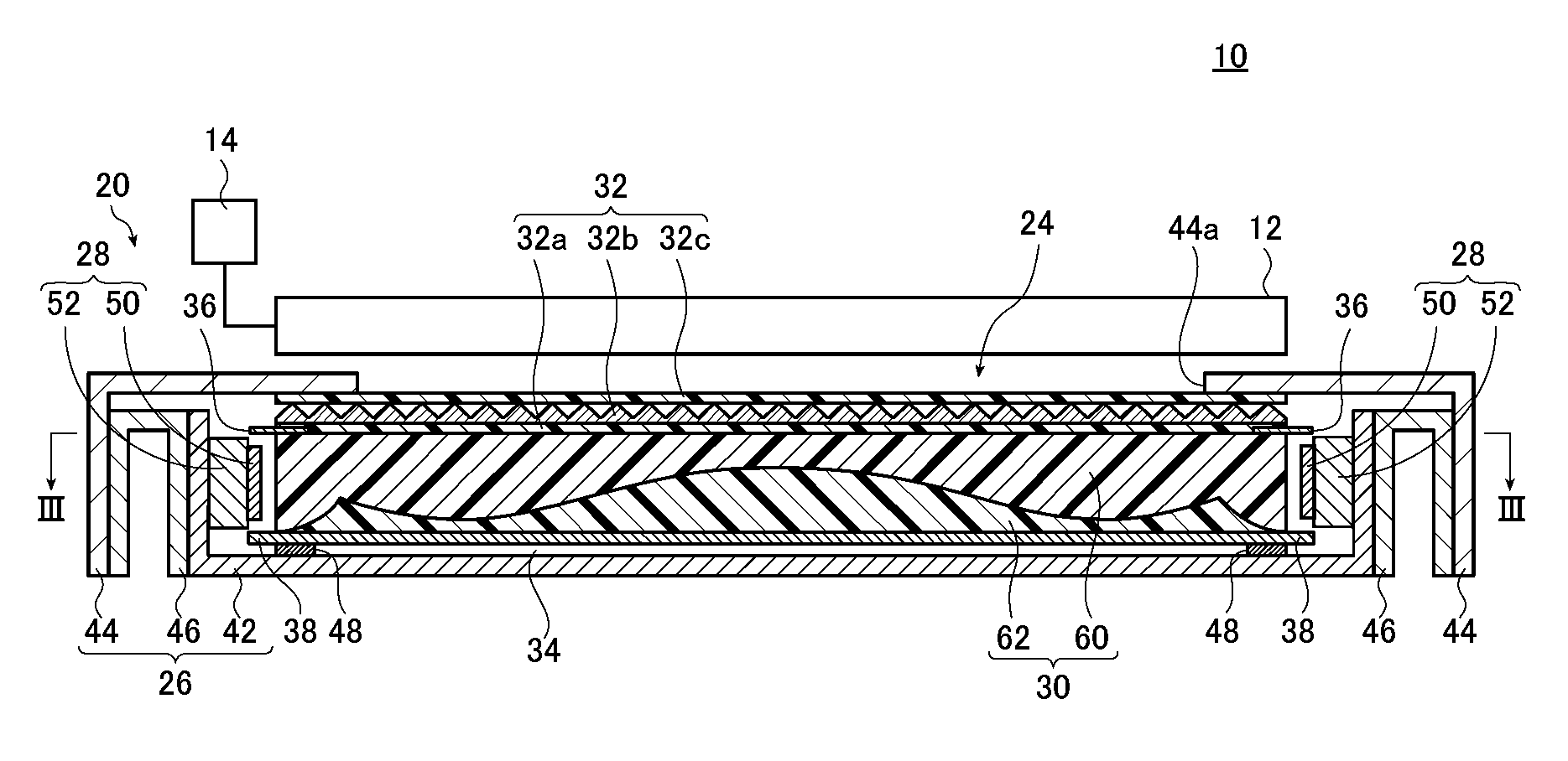
[0210]In Example 1, the illuminance distribution and luminance distribution of outgoing light through the light exit surface were determined by computer simulation using a light guide plate having the interface z as shown in FIG. 6.
[0211]In the simulation, the material of the transparent resin of the light guide plate and the material of the scattering particles were modeled as PMMA and silicone, respectively. This will also apply to all the examples given below.
[0212]In Example 1, the light guide plate 150 corresponding to a 40-inch screen size was used.
[0213]More specifically, the length from the first light incidence surface 30c to the third light incidence surface 30d was set to 539 mm; the length from the second light incidence surface 30f to the fourth light incidence surface 30g to 922 mm; and the thickness to 1.5 mm.
[0214]The scattering particles to be kneaded and dispersed in the light guide plate had a center particle size of 4.5 μm.
[0215]The second layer had a thickness s...
example 2
[0221]A light guide plate of the same type as that used in Example 1 except the shape of the interface z was used to measure the illuminance distribution.
[0222]The second layer of the light guide plate 150 in Example 2 had the thickness shape shown in FIG. 11.
[0223]More specifically, in the cross section perpendicular to the longitudinal direction of the first light incidence surface 30c which is formed in the central portion between the second light incidence surface 30f and the fourth light incidence surface 30g, the thickness of the second layer 154 at the position of the second local maximum value was set to 0.8 mm; the thickness of the second layer 154 at the positions of the first local maximum value (on the light incidence surfaces) to 0.15 mm; the thickness of the second layer 154 at the thinnest positions to 0.14 mm; and the distance from the central portion of the light guide plate to the thinnest positions to 246.5 mm.
[0224]In the cross section perpendicular to the longit...
reference example 1
[0227]In Reference Example 1, a backlight unit 200 shown in FIGS. 14A to 14C was used.
[0228]The backlight unit 200 shown in FIGS. 14A to 14C has a configuration in which light sources are disposed on two opposite surfaces of the light guide plate, whereas light sources are not disposed on the other two opposite surfaces.
[0229]A light guide plate 202 of the backlight unit 200 includes a first layer 204 on the side closer to a light exit surface and a second layer 206 on the side closer to a rear surface. When seen in a cross section perpendicular to the longitudinal direction of surfaces on the sides on which light sources are disposed (light incidence surfaces), an interface z between the first layer 204 and the second layer 206 continuously changes so that the second layer 206 decreases in thickness from the central portion of the light exit surface toward the two light incidence surfaces, and further continuously changes so that the second layer 206 increases in thickness in the v...
PUM
 Abstract
Description
Claims
Application Information


