Manufacturing apparatus and method for large-scale production of thin-film solar cells

a solar cell and manufacturing apparatus technology, applied in the field of photovoltaics, can solve the problems of not working for cigs at its normal processing temperature, application at relatively low process temperature, and general poor conductivity and reflectivity of alloys, so as to improve the back contact/reflection layer, reduce the cost, and eliminate cadmium

Active Publication Date: 2005-05-26
BEIJING APOLLO DING RONG SOLAR TECH
View PDF19 Cites 309 Cited by
  • Summary
  • Abstract
  • Description
  • Claims
  • Application Information

AI Technical Summary

Benefits of technology

[0027] A primary objective of the present invention is to provide a large-scale manufacturing system for the economical production of thin-film CIGS solar cells.
[0028] An additional objective of the invention is to provide a manufacturing protocol for solar cells in which high temperature toxic gases and toxic wet chemical baths are eliminated from the process.
[0029] Another objective of the invention is to provide a manufacturing process for CIGS solar cells, which significantly lowers thei...

Problems solved by technology

A limitation to use of these alloys is that they must be applied at relatively low process temperatures, below about 120 C., which are marginally appropriate for amorphous silicon absorber layers, but would not work for CIGS at its normal processing temperatures.
When it is placed against t...

Method used


Image

  • Manufacturing apparatus and method for large-scale production of thin-film solar cells
  • Manufacturing apparatus and method for large-scale production of thin-film solar cells
  • Manufacturing apparatus and method for large-scale production of thin-film solar cells

Examples


Embodiment Construction

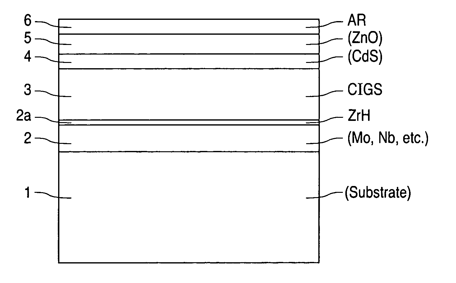
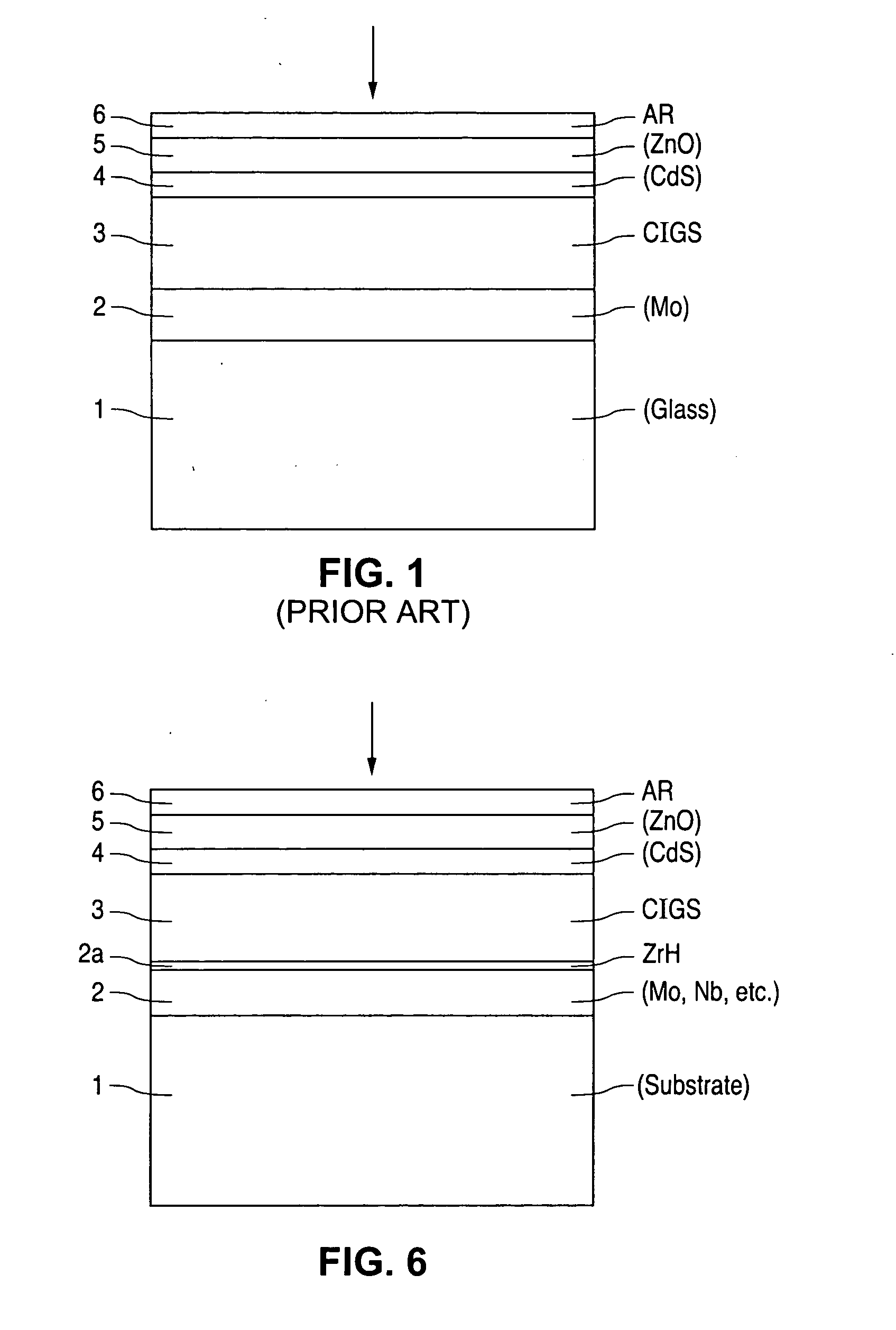
[0052] The invention will now be described and compared with respect to the conventional prior art CIGS solar cell structure. The new cell structure and the manufacturing process will be detailed in relation to a modular roll-to-roll sputter deposition system designed specifically to provide an optimum implementation of the process.

[0053] It should be noted that, as used herein, the terms “over” and “on” both inclusively include “directly on” (no intermediate materials, elements or space disposed therebetween) and “indirectly on” (intermediate materials, elements or space disposed therebetween). For example, forming an element “on a substrate” can include forming the element directly on the substrate with no intermediate materials / elements therebetween, as well as forming the element indirectly on the substrate with one or more intermediate materials / elements therebetween.

[0054]FIG. 6 illustrates one of the simplest embodiments of a basic solar cell according to the present invent...


PUM

PropertyMeasurementUnit
Fractionaaaaaaaaaa
Fractionaaaaaaaaaa
Fractionaaaaaaaaaa

Abstract

A method of manufacturing improved thin-film solar cells entirely by sputtering includes a high efficiency back contact/reflecting multi-layer containing at least one barrier layer consisting of a transition metal nitride. A copper indium gallium diselenide (Cu(InXGa1-x)Se2) absorber layer (X ranging from 1 to approximately 0.7) is co-sputtered from specially prepared electrically conductive targets using dual cylindrical rotary magnetron technology. The band gap of the absorber layer can be graded by varying the gallium content, and by replacing the gallium partially or totally with aluminum. Alternately the absorber layer is reactively sputtered from metal alloy targets in the presence of hydrogen selenide gas. RF sputtering is used to deposit a non-cadmium containing window layer of ZnS. The top transparent electrode is reactively sputtered aluminum doped ZnO. A unique modular vacuum roll-to-roll sputtering machine is described. The machine is adapted to incorporate dual cylindrical rotary magnetron technology to manufacture the improved solar cell material in a single pass.

Description

[0001] This application claims the benefit of U.S. Provisional Application No. 60 / 415,009, filed Sep. 30, 2002; and of U.S. Provisional Application No. 60 / 435,814, filed Dec. 19, 2002.FIELD OF THE INVENTION [0002] The invention disclosed herein relates generally to the field of photovoltaics, and more specifically to a unique high throughput roll-to-roll vacuum deposition system and method for the manufacturing of thin-film solar cells based upon absorbing layers that contain copper, indium, gallium, aluminum, and selenium and have a polycrystalline chalcopyrite structure. BACKGROUND OF THE INVENTION [0003] Interest in thin-film photovoltaics has expanded in recent years. This is due primarily to improvements in conversion efficiency of cells made at the laboratory scale, and the anticipation that manufacturing costs can be significantly reduced compared to the older and more expensive crystalline and polycrystalline silicon technology. The term “thin-film” is used to distinguish th...

Claims


Application Information

Patent Timeline
IPC IPC(8): C23C14/00C23C14/35C23C14/56H01L31/032
CPCC23C14/0057C23C14/352C23C14/562H01L31/022425H01L31/18H01L31/0336Y02E10/541C23C14/3414H01L31/0322Y02P70/50
Inventor HOLLARS, DENNIS R.
Owner BEIJING APOLLO DING RONG SOLAR TECH
Why Eureka
Try Eureka