Supercharge Your Innovation With Domain-Expert AI Agents!

Semiconductor wafers, and testing methods thereof

Active Publication Date: 2016-06-28
WINBOND ELECTRONICS CORP
View PDF8 Cites 0 Cited by
  • Summary
  • Abstract
  • Description
  • Claims
  • Application Information

AI Technical Summary

Benefits of technology

The invention is a semiconductor wafer with a die area and a scribe area. The die has a main circuit and a testing circuit, which is connected to the die for testing its main circuit. The testing circuit can communicate with the main circuit through a seal ring and a well. The testing circuit can also encrypt and decrypt test data, and use a non-volatile memory fuse to store values for determining the function of the main circuit. The invention provides a testing method for the semiconductor wafer, which can speed up the testing process and ensure more reliable connections between the circuit components.

Problems solved by technology

However, a hacker may uses the test interface to steal information from the integrate circuit of the die, it may be insecure.

Method used


Image

  • Semiconductor wafers, and testing methods thereof
  • Semiconductor wafers, and testing methods thereof
  • Semiconductor wafers, and testing methods thereof

Examples


Embodiment Construction

[0022]Several exemplary embodiments of the application are described with reference to drawings, which generally relate to navigation of a movable platform. It is to be understood that the following disclosure provides various different embodiments as examples for implementing different features of the application. Specific examples of components and arrangements are described in the following to simplify the present disclosure. These are, of course, merely examples and are not intended to be limiting. In addition, the present disclosure may repeat reference numerals and / or letters in the various examples. This repetition is for the purpose of simplicity and clarity and does not in itself dictate a relationship between the various described embodiments and / or configurations.

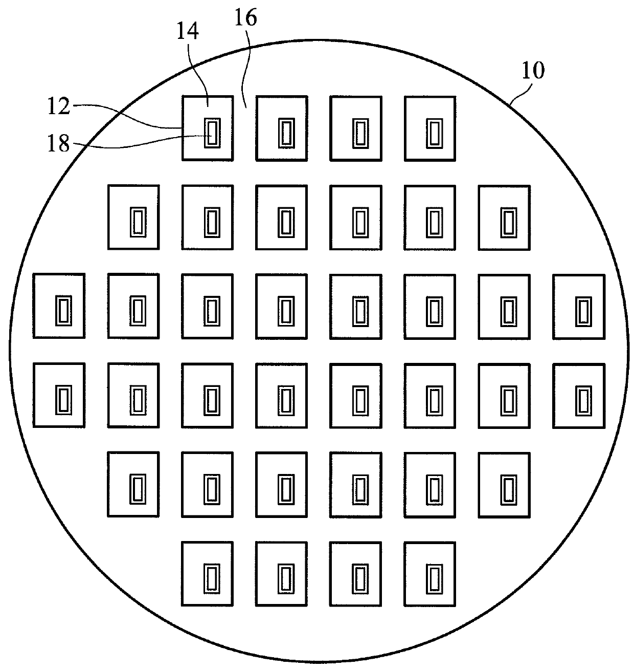
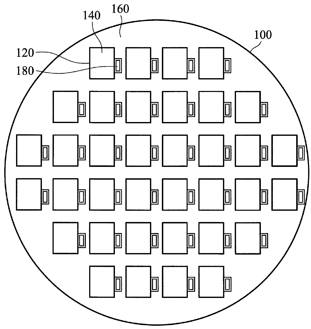
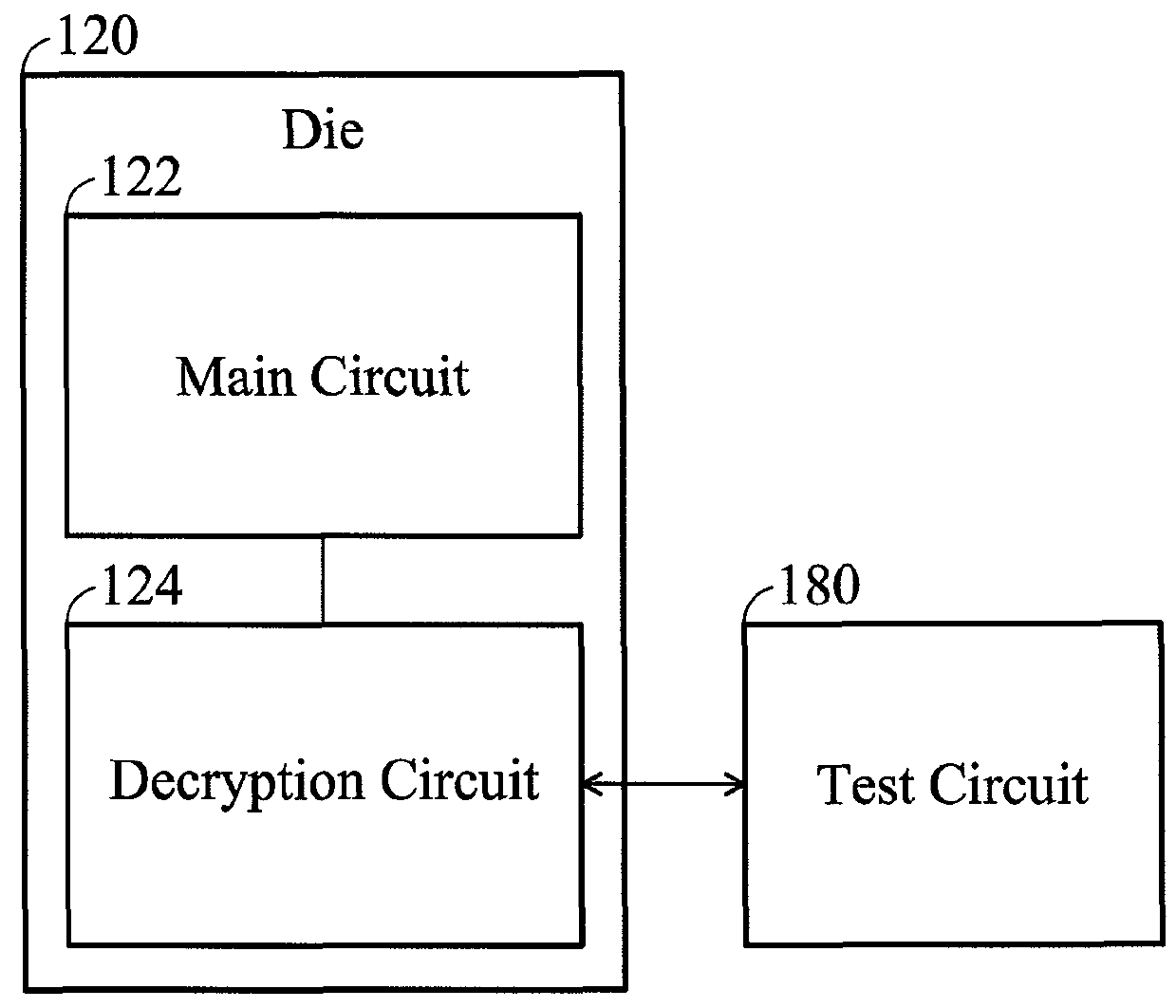
[0023]FIG. 2 is a top view of a semiconductor wafer including multiple dies and test circuits in accordance with an embodiment of the present invention. In the embodiment, the semiconductor wafer 100 comprises mu...


PUM


Abstract

The invention provides a semiconductor wafer with a die area and a scribe area, and the semiconductor wafer includes a die and a testing circuit. The die is formed on the die region of the semiconductor wafer, and the die includes a main circuit. The testing circuit is disposed on the scribe area of the semiconductor wafer, and is electrically connected to the die for testing the main circuit.

Description

BACKGROUND OF THE INVENTION[0001]1. Field of the Invention[0002]The present invention relates to semiconductor wafers, and more particularly to a semiconductor wafer having an off-chip testing circuit for testing a die.[0003]2. Description of the Related Art[0004]Nowadays, in a conventional semiconductor wafer manufacturing process, an integrated circuit formed in a die (also as a chip) needs to be tested for functionality, process integrity, device behavior, and reliability, etc. FIG. 1 shows a top view of a conventional semiconductor wafer 10, the semiconductor wafer 10 comprises a plurality of dies 12 formed on die areas 14 of the semiconductor wafer 10, and the other area on the semiconductor wafer may be defined as a scribe area 16. Also, in a conventional semiconductor wafer 10, a testing circuit 18 for testing the integrated circuit of the die is also formed in the die within the die areas 14. However, because the testing circuit 18 is embodied in the die, the size of the die...

Claims


Application Information

Patent Timeline
Patent Type & Authority Patents(United States)
IPC IPC(8): G01R31/26G09C1/00G01R31/28
CPCG01R31/2607G01R31/2884G09C1/00H04L2209/12G01R31/318511
Inventor HUNG, HSI-HSIENCHAN, JOHNNYCHENG, DENNIS
Owner WINBOND ELECTRONICS CORP
Features
  • R&D
  • Intellectual Property
  • Life Sciences
  • Materials
  • Tech Scout
  • Unparalleled Data Quality
  • Higher Quality Content
  • 60% Fewer Hallucinations
Learn More