Array substrate, method of manufacturing array substrate and display device

a technology of array substrate and array substrate, which is applied in the field of array substrate, can solve the problems of array substrate having a worse display performance, prone to oxidation, and large so as to reduce or eliminate oxidation of copper metal layer, and avoid influence on display characteristics

Active Publication Date: 2016-11-29
BOE TECH GRP CO LTD
View PDF3 Cites 1 Cited by
  • Summary
  • Abstract
  • Description
  • Claims
  • Application Information

AI Technical Summary

Benefits of technology

[0040]Embodiments of the present invention provides an array substrate, a method of manufacturing an array substrate and a display device, which avoid the copper metal layer from being completely exposed to an oxygen enriched environment to be oxidized and ensure the copper metal layer to be not in contact with the silicon oxide layer, thereby reducing or eliminating oxidation of the copper metal layer, by firstly forming the passivation layer on the source-drain metal pattern and then forming the oxide trench pattern, and by further modifying the structure of the passivation layer to include the silicon nitride layer as the lower layer and the silicon oxide layer as the upper layer. Further, it may ensure the oxide trench pattern to be not in contact with the silicon oxide layer, avoid influence on display characteristic of the array substrate, and thus reduce or eliminate oxidation of the copper metal layer and improve display performance of the array substrate, by forming the trench in the passivation layer at a position corresponding to the gap between the source electrode and the drain electrode, such that the width of the trench in the silicon oxide layer is smaller than the width of the trench in the silicon nitride layer and is larger than or equal to the width of the gap between the source electrode and the drain electrode.

Problems solved by technology

However, as the oxide trench pattern 1005 is located on the upper copper metal layer, the copper metal layer is completely exposed to an oxygen enriched environment and thus tends to be oxidized.
In this instance, the copper metal layer will be oxidized to a large extent and the array substrate has a worse display performance.

Method used


Image

  • Array substrate, method of manufacturing array substrate and display device
  • Array substrate, method of manufacturing array substrate and display device
  • Array substrate, method of manufacturing array substrate and display device

Examples


Embodiment Construction

[0056]Embodiments of the present invention will be further described in detail in combination with drawings in order that objects, technical schemes and advantages of the present invention will be more explicit.

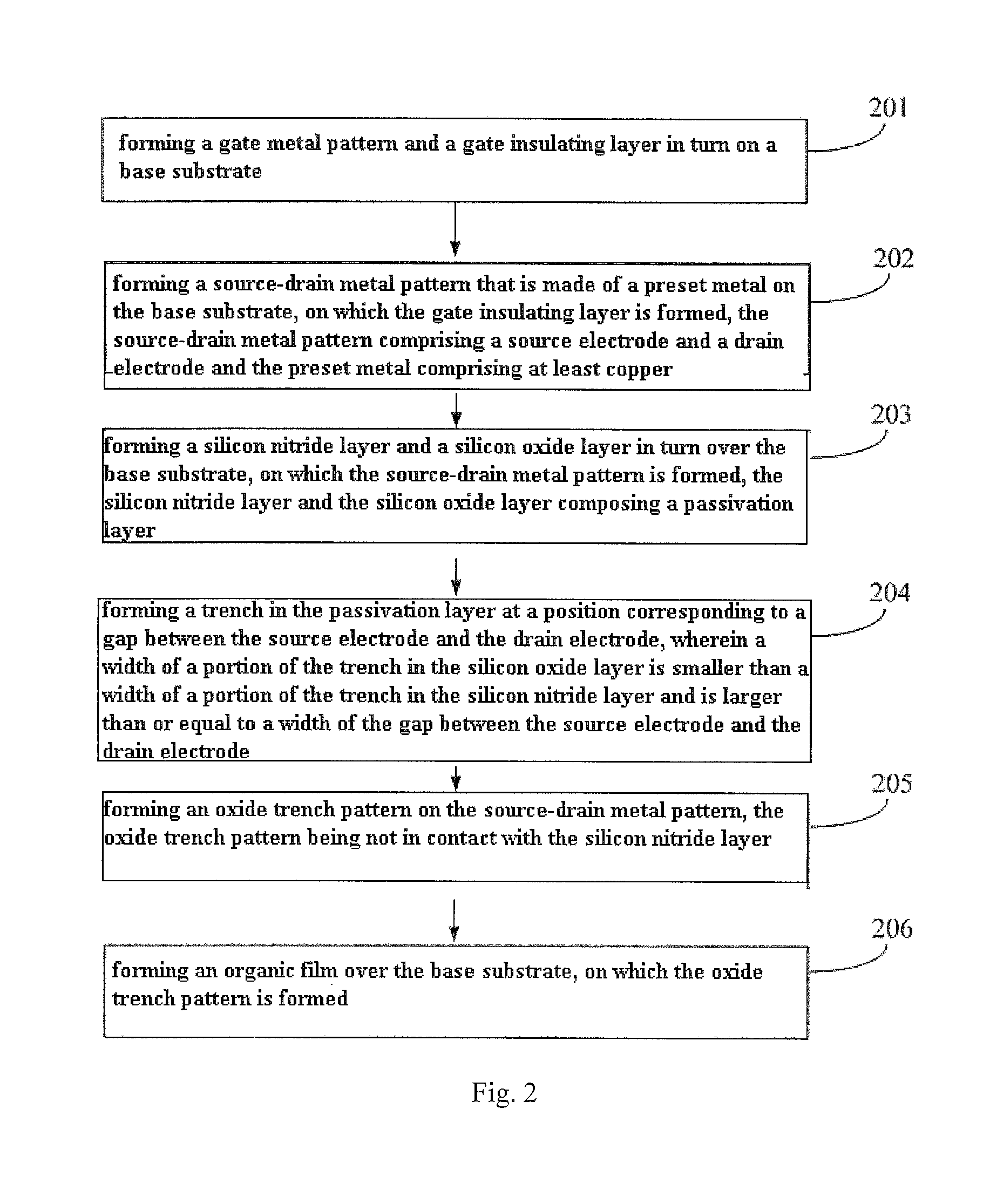
[0057]Embodiments of the present invention provide a method of manufacturing an array substrate, as shown in FIG. 2, the method comprising:

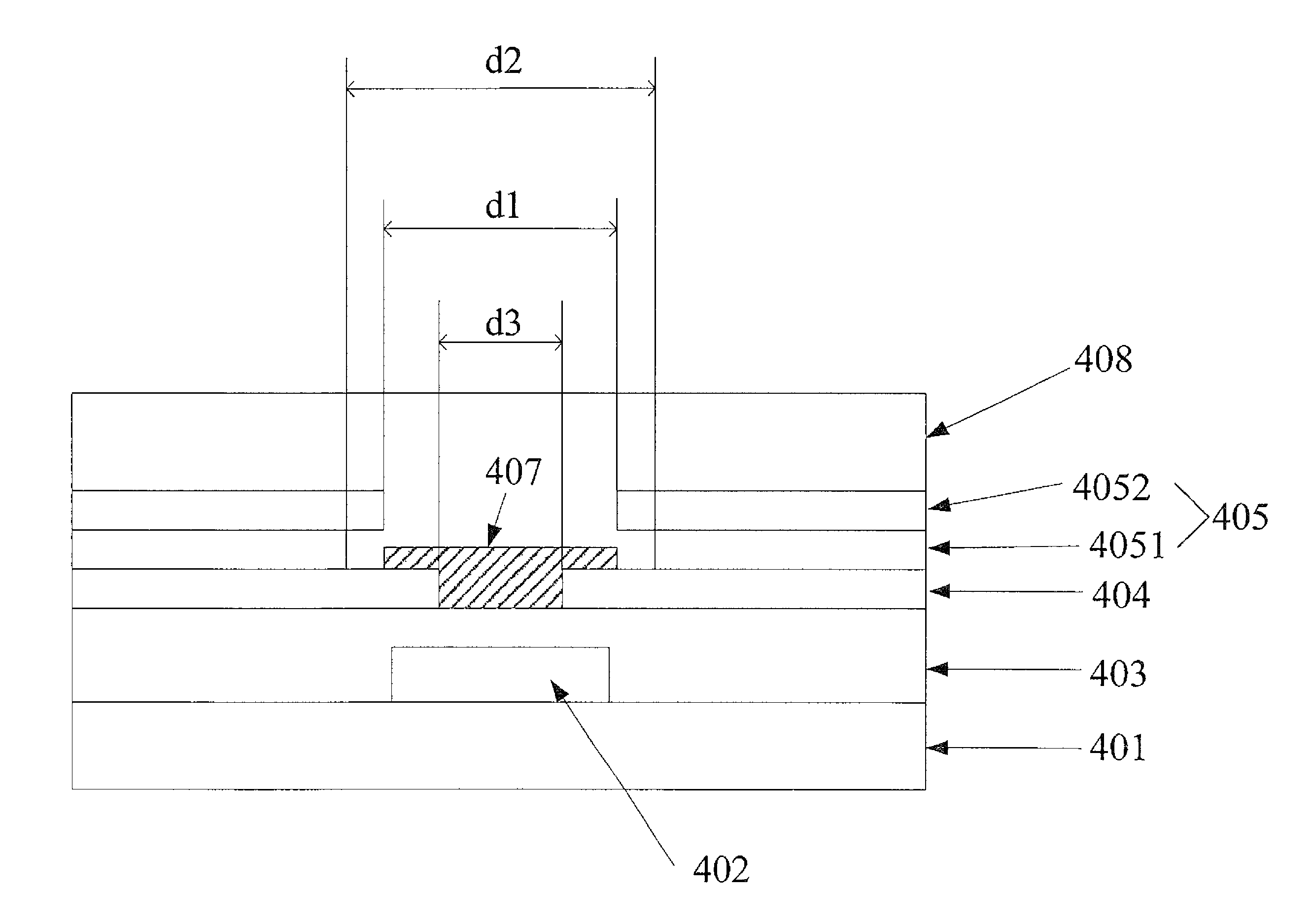
[0058]Step 201: forming a gate metal pattern and a gate insulating layer in turn on a base substrate;

[0059]Step 202: forming a source-drain metal pattern that is made of a preset metal on the base substrate, on which the gate insulating layer is formed, the source-drain metal pattern comprising a source electrode and a drain electrode and the preset metal comprising at least copper;

[0060]Step 203: forming a silicon nitride layer and a silicon oxide layer in turn over the base substrate, on which the source-drain metal pattern is formed, the silicon nitride layer and the silicon oxide layer composing a passivation layer;

[0061]Step 204: form...


PUM

PropertyMeasurementUnit
widthaaaaaaaaaa
sizeaaaaaaaaaa
wire resistanceaaaaaaaaaa

Abstract

Embodiments of the present invention disclose an array substrate, a method of manufacturing an array substrate and a display device, which belong to field of display technology. The method includes: forming a gate metal pattern and a gate insulating layer in turn on a base substrate; forming a source-drain metal pattern that is made of a preset metal on the base substrate, on which the gate insulating layer is formed, the source-drain metal pattern comprising a source electrode and a drain electrode and the preset metal including at least copper; forming a silicon nitride layer and a silicon oxide layer in turn on the base substrate, which compose a passivation layer; forming a trench in the passivation layer at a position corresponding to a gap between the source electrode and the drain electrode, wherein a width of the trench in the silicon oxide layer is smaller than a width of the trench in the silicon nitride layer and is larger than or equal to a distance of the gap between the source electrode and the drain electrode; forming an oxide trench pattern on the source-drain metal pattern, with is not in contact with the silicon nitride layer. The present invention solves problems of high-degree oxidation of copper metal layer and poorer display performance of an existing array substrate, and achieves advantages of reducing oxidation of copper metal layer and improving display performance of the array substrate for a display device.

Description

CROSS-REFERENCE TO RELATED APPLICATIONS[0001]This application claims priority of Chinese Application No. 201510171291.5, filed Apr. 10, 2015, entitled “Array Substrate, Method of Manufacturing Array Substrate and Display Device”, which is incorporated herein by reference in their entirety.BACKGROUNDTechnical Field[0002]The invention relates to field of display technology, and particularly to an array substrate, a method of manufacturing the array substrate and a display device.Description of the Related Art[0003]Organic Light-Emitting Diode (OLED) is a current mode semiconductor Light-Emitting device based on an organic material. Recently, a display device which is characterized in including OLED has been developed to have a large size, a high resolution and a fast response. In order to reduce cost and improve displaying quality of a display panel, an oxide thin film transistor (TFT) array substrate, which is formed in a copper+oxide coplanar structure, is approached. As copper is u...

Claims


Application Information

Patent Timeline
Patent Type & Authority Patents(United States)
IPC IPC(8): H01L21/00H01L27/12H01L29/49H01L29/45H01L21/475H01L21/471H01L21/473H01L29/06H01L29/786H01L29/66
CPCH01L27/1296H01L21/471H01L21/473H01L21/475H01L27/1225H01L29/0649H01L29/45H01L29/495H01L29/66969H01L29/78693H01L29/78636H01L29/7869H01L27/1248H10K99/00
Inventor LIU, WEIJIANG, CHUNSHENG
Owner BOE TECH GRP CO LTD
Why Eureka
Try Eureka