Flexible packages including chips

Active Publication Date: 2017-03-28
SK HYNIX INC
View PDF10 Cites 6 Cited by
  • Summary
  • Abstract
  • Description
  • Claims
  • Application Information

AI Technical Summary

Problems solved by technology

In general, if a warped semiconductor chip is attached to another semiconduc

Method used


Image

  • Flexible packages including chips
  • Flexible packages including chips
  • Flexible packages including chips

Examples


Example

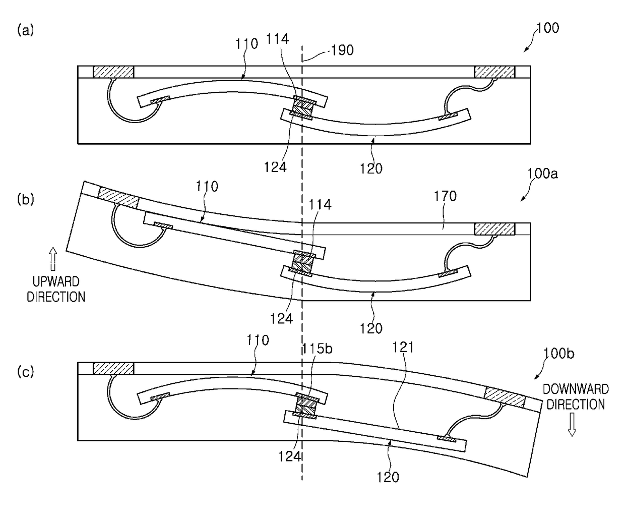
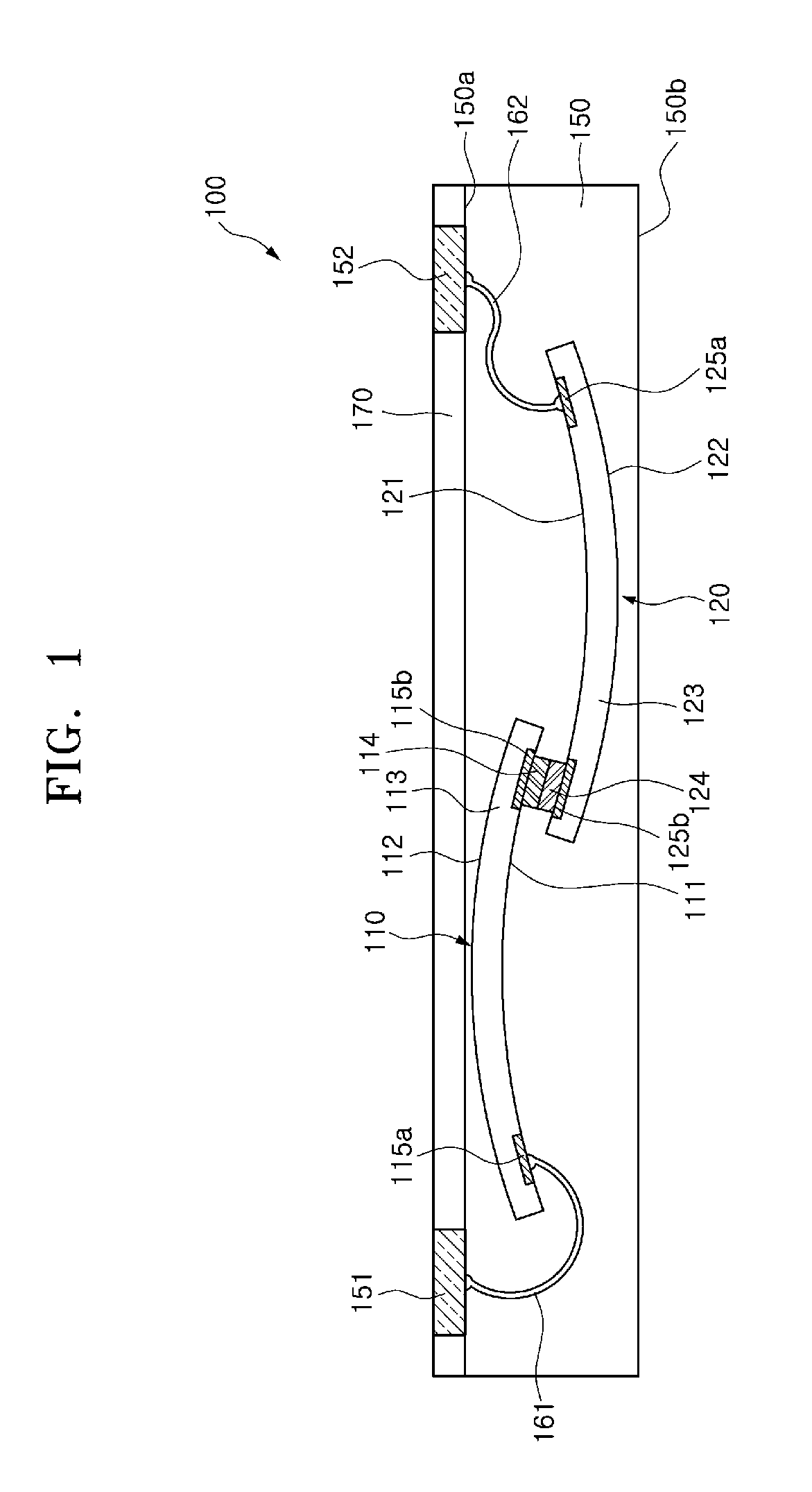
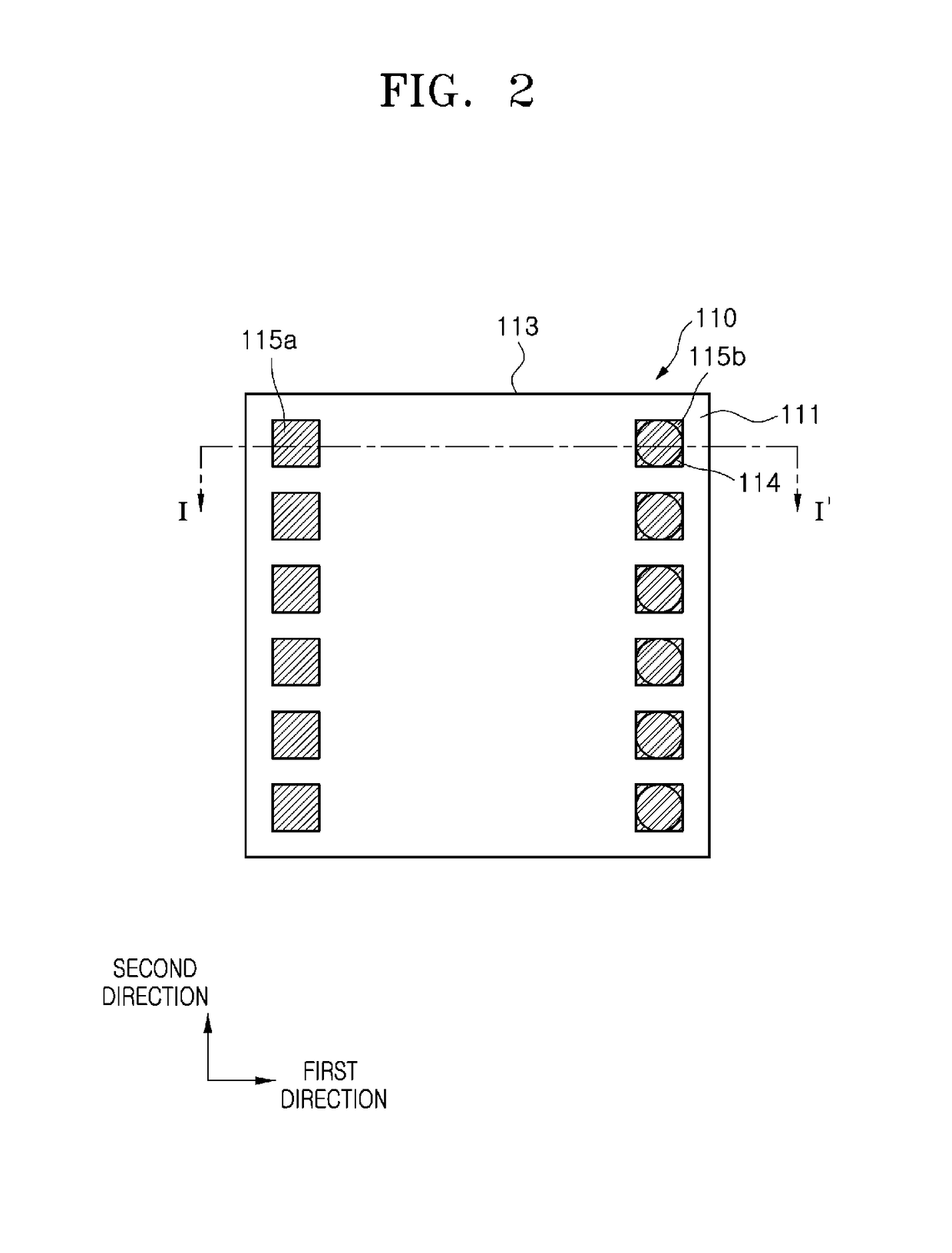
[0026]It will be understood that although the terms first, second, third etc. may be used herein to describe various elements, these elements should not be limited by these terms. These terms are only used to distinguish one element from another element. Thus, a first element in some embodiments could be termed a second element in other embodiments without departing from the teachings of the present disclosure.

[0027]It will also be understood that when an element is referred to as being located “on,”“over,”“above,”“under,”“beneath,”“below,”“side,” or “aside” another element, it may directly contact the other element, or at least one intervening element may be present therebetween. Accordingly, the terms such as “on,”“over,”“above,”“under,”“beneath,”“below,”“side,”“aside,” and the like that are used herein are for the purpose of describing only a position relationship of two elements and are not intended to limit the scope of the present disclosure.

[0028]It will be further understood...


PUM


Abstract

A flexible package may be provided. The flexible package may include a flexible molding member including a top surface. The flexible package may include a first chip within the flexible molding member, and including a first top surface. The flexible package may include a second chip within the flexible molding member, and including a second top surface. The first top surface may face away from the top surface of the flexible molding member and the second top surface may face towards the top surface of the flexible molding member.

Description

CROSS-REFERENCE TO RELATED APPLICATION[0001]The present application claims priority under 35 U.S.C. 119(a) to Korean Patent Application No. 10-2015-0164756, filed on Nov. 24, 2015, which is herein incorporated by references in its entirety.BACKGROUND[0002]1. Technical Field[0003]Various embodiments of the present disclosure generally relate to packages and, more particularly, to flexible packages including chips.[0004]2. Related Art[0005]Semiconductor packages capable of processing a large amount of data are increasingly in demand with the development of smaller electronic systems such as mobile systems. As the electronic systems become lighter and smaller, the semiconductor packages employed in the electronic systems have been continuously scaled down. In addition, flexible electronic systems which are capable of bending or warping are increasingly in demand with increase of the interest in portable and wearable electronic systems.[0006]Meanwhile, semiconductor chips employed in se...

Claims


Application Information

Patent Timeline
IPC IPC(8): H01L23/498H01L23/31H01L25/065
CPCH01L25/0657H01L23/3121H01L23/4985H01L2225/06513H01L2225/0651H01L2225/06565H01L23/488H01L24/09H01L24/17H01L25/00H01L2224/091H01L2224/171H01L2224/17104H01L23/3107H01L23/49811H01L23/562H01L24/06H01L24/13H01L24/14H01L24/16H01L24/48H01L24/73H01L25/0652H01L2224/0401H01L2224/04042H01L2224/05554H01L2224/06155H01L2224/13294H01L2224/133H01L2224/14155H01L2224/14165H01L2224/16145H01L2224/48091H01L2224/48105H01L2224/48247H01L2224/48464H01L2224/73207H01L2225/06555H01L2225/06582H01L2924/00014H01L2924/1015H01L2924/181H01L2924/3511H01L2924/00012H01L2224/45099H01L23/08H01L23/293H01L2225/06517
Inventor JEONG, CHAN WOO
Owner SK HYNIX INC
Why Eureka
Try Eureka