Vertical floating gate memory with variable channel doping profile

Inactive Publication Date: 2017-10-03
IBM CORP
View PDF6 Cites 13 Cited by
  • Summary
  • Abstract
  • Description
  • Claims
  • Application Information

AI Technical Summary

Benefits of technology

The patent describes a method and structure for fabricating a memory device with improved performance. The method involves forming a channel region with different dopant concentrations, to optimize current flow and improve the device's ability to store information. Additionally, the method includes the use of a sacrificial gate to facilitate the formation of a separate source and drain region, which helps to improve the device's stability and performance. The resulting memory device includes a source region, drain region, and an epitaxial channel region with a modulated dopant concentration that enhances the device's ability to store information. The device also includes a memory gate structure, which includes a floating gate and a control gate. Overall, the patent provides technical improvements for memory devices that lead to better performance and stability.

Problems solved by technology

With ever decreasing device dimensions, forming the individual electrical components is becoming more difficult to manufacture.
Integration of memory devices with increasingly scaled transistors, such as vertical transistors, creates additional challenges.

Method used


Image

  • Vertical floating gate memory with variable channel doping profile
  • Vertical floating gate memory with variable channel doping profile
  • Vertical floating gate memory with variable channel doping profile

Examples


Embodiment Construction

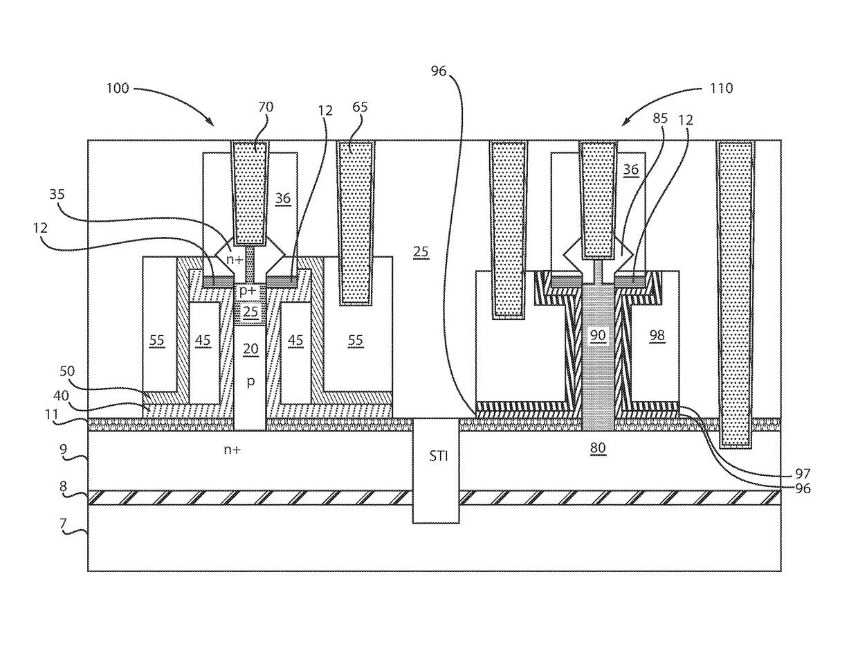
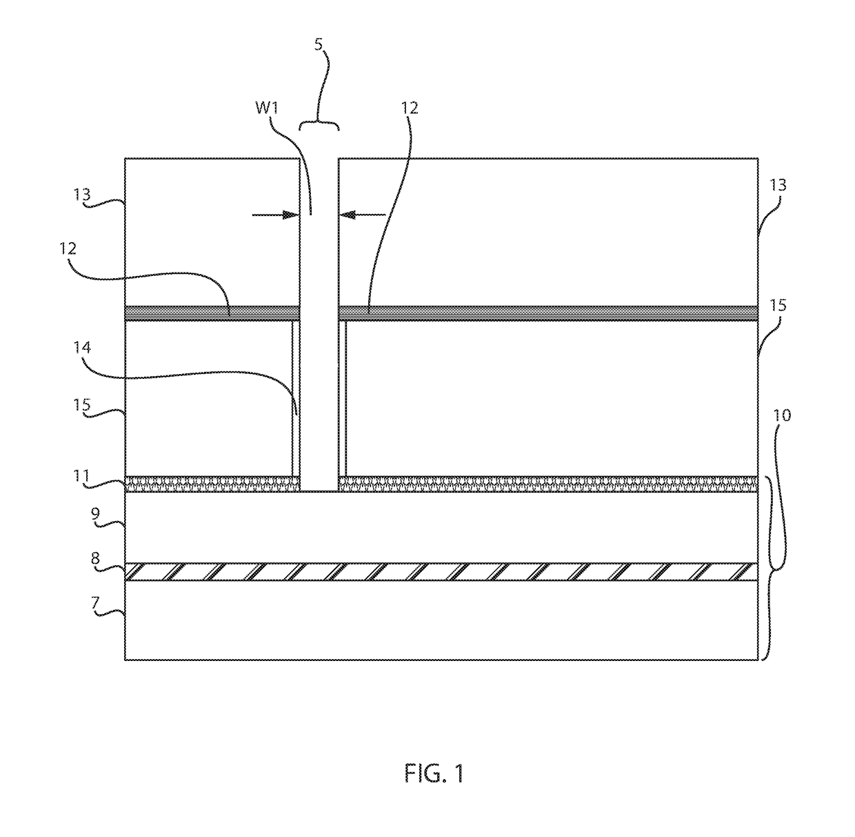
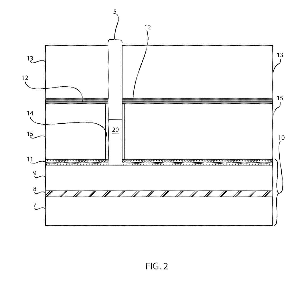
[0027]Detailed embodiments of the claimed structures and methods are disclosed herein; however, it is to be understood that the disclosed embodiments are merely illustrative of the claimed structures and methods that may be embodied in various forms. In addition, each of the examples given in connection with the various embodiments is intended to be illustrative, and not restrictive. Further, the figures are not necessarily to scale, some features may be exaggerated to show details of particular components. Therefore, specific structural and functional details disclosed herein are not to be interpreted as limiting, but merely as a representative basis for teaching one skilled in the art to variously employ the methods and structures of the present disclosure. For purposes of the description hereinafter, the terms “upper”, “lower”, “right”, “left”, “vertical”, “horizontal”, “top”, “bottom”, and derivatives thereof shall relate to the embodiments of the disclosure, as it is oriented i...


PUM


Abstract

A method of forming a memory device that includes forming a sacrificial gate on a surface of a first source / drain region, and forming a channel opening through the sacrificial gate. The method may further include forming an epitaxial channel region is formed in the channel opening that is in situ doped to have an opposite conductivity type as the first of the source / drain region. A second source / drain region is formed on a portion of the epitaxial channel region opposite the portion of the epitaxial channel region that the first source / drain region is present on, wherein the second source / drain region has a same conductivity type as the conductivity type of the first source / drain region. A memory gate structure including a floating gate and a control gate is substituted for the sacrificial gate.

Description

BACKGROUND[0001]Technical Field[0002]The present disclosure relates to vertically orientated memory devices, and methods of forming vertical memory devices. The methods and structures described herein integrate vertical field effect transistors with vertically orientated memory devices that include a floating gate.[0003]Description of the Related Art[0004]A Field Effect Transistor (FET) typically has a source, a channel, and a drain, where current flows from the source to the drain, and a gate that controls the flow of current through the channel. With ever decreasing device dimensions, forming the individual electrical components is becoming more difficult to manufacture. Vertical transistors are one means of scaling transistors to decreasing dimensions. Integration of memory devices with increasingly scaled transistors, such as vertical transistors, creates additional challenges. An approach is therefore needed that retains the positive aspects of traditional FET structures and me...

Claims


Application Information

Patent Timeline
IPC IPC(8): H01L27/11521H01L29/66H01L21/02H01L21/28H01L29/10H01L29/78H01L29/788H01L29/165H01L29/08
CPCH01L27/11521H01L29/66545H01L29/66825H01L29/66666H01L21/02573H01L21/28273H01L29/1037H01L29/7827H01L29/788H01L29/165H01L29/0847H01L28/00H10B43/27
Inventor BALAKRISHNAN, KARTHIKHASHEMI, POUYANING, TAK H.REZNICEK, ALEXANDER
Owner IBM CORP
Why Eureka
Try Eureka