Memory devices and methods of manufacturing the same

a technology of memory devices and memory storage, applied in the direction of semiconductor devices, electrical equipment, transistors, etc., can solve the problems of long distance between the electrodes or holes, and achieve the effects of longer data retention time, faster data programming/erasing speed, and higher endurance capacity

Inactive Publication Date: 2008-07-10
SAMSUNG ELECTRONICS CO LTD
View PDF5 Cites 2 Cited by
  • Summary
  • Abstract
  • Description
  • Claims
  • Application Information

AI Technical Summary

Benefits of technology

[0036]According to some exemplary embodiments of the present invention, a first tunnel insulation layer pattern, which has a first thickness smaller than that of a conventional tunnel insulation layer pattern, and a second tunnel insulation layer pattern, which has an energy band gap smaller than that of the first tunnel insulation layer pattern, are formed on a semiconductor substrate. Thus, a memory device including the first and second tunnel insulation layer patterns in accordance with exemplary embodiments of the present invention may have improved characteristics such as, for example, faster data programming / erasing speeds because the probability that electrons and holes move between a charge trapping layer pattern and a channel region in the semiconductor substrate may be increased while programming or erasing data.
[0037]Additionally, a probability that charges trapped in the charge trapping layer pattern move to the semiconductor substrate according as time elapses may be decreased because a total thickness of the first thickness and a second thickness, e.g., the thickness of the second tunnel insulation layer pattern, may be larger than that of the conventional tunnel insulation layer pattern. Thus, the memory device according to exemplary embodiments of the present invention may have improved characteristics such as, for example, a longer data retention time or a higher endurance capacity to a high temperature stress.

Problems solved by technology

However, when the tunnel insulation layer has a large thickness, electrons or holes may move along a long distance while programming or erasing data.

Method used


Image

  • Memory devices and methods of manufacturing the same
  • Memory devices and methods of manufacturing the same
  • Memory devices and methods of manufacturing the same

Examples


Embodiment Construction

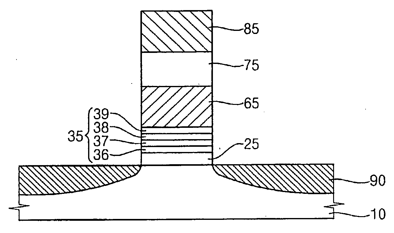
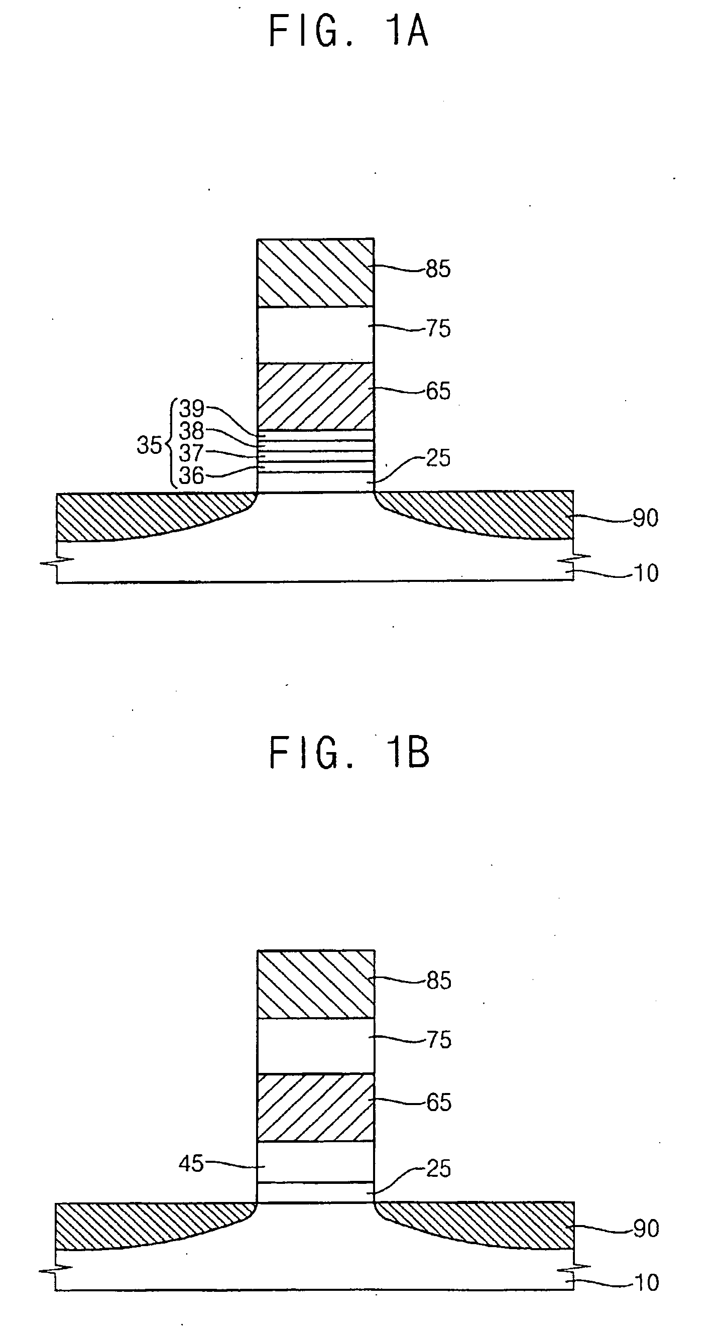
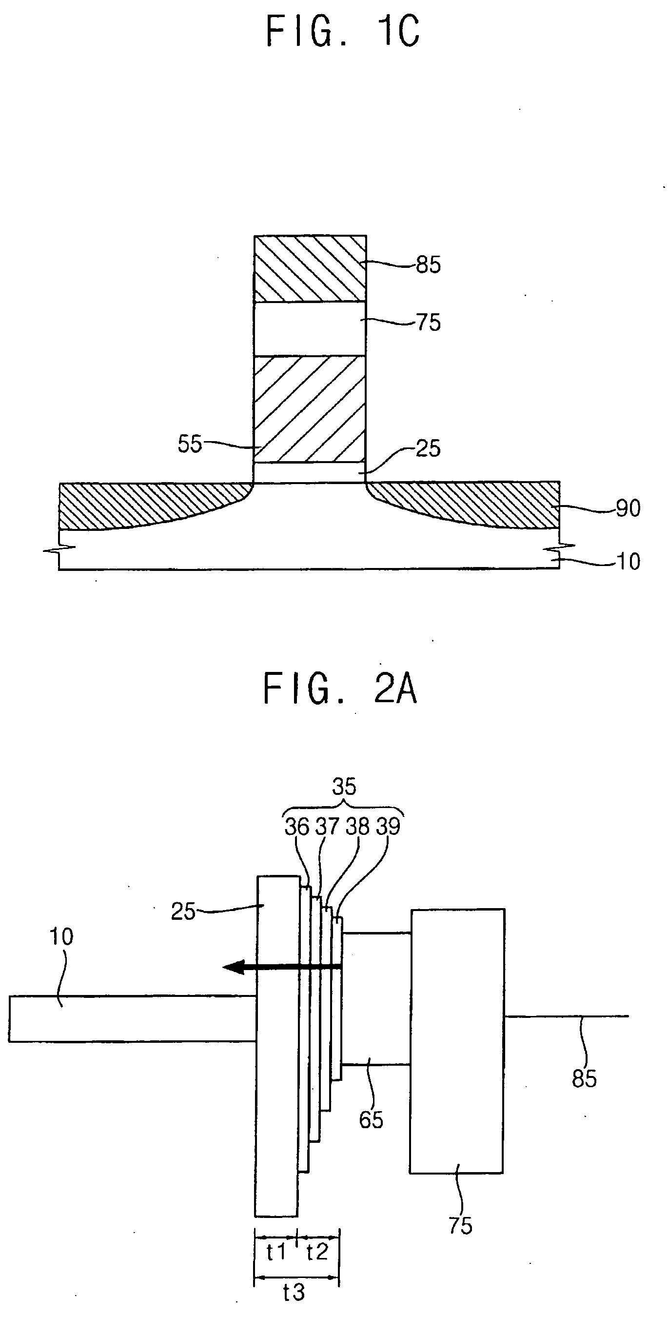
[0046]The present invention is described more fully hereinafter with reference to the accompanying drawings, in which exemplary embodiments of the present invention are shown. The present invention may, however, be embodied in many different forms and should not be construed as limited to the exemplary embodiments set forth herein. In the drawings, the sizes and relative sizes of layers and regions may be exaggerated for clarity.

[0047]It will be understood that when an element or layer is referred to as being “on,”“connected to” or “coupled to” another element or layer, it can be directly on, connected or coupled to the other element or layer or intervening elements or layers may be present. In contrast, when an element is referred to as being “directly on,”“directly connected to” or “directly coupled to” another element or layer, there are no intervening elements or layers present. Like numerals refer to like elements throughout. As used herein, the term “and / or” includes any and a...


PUM


Abstract

The memory device includes a first tunnel insulation layer pattern on a semiconductor substrate, a second tunnel insulation layer pattern having an energy band gap lower than that of the first tunnel insulation layer pattern on the first tunnel insulation layer pattern, a charge trapping layer pattern on the second tunnel insulation layer pattern, a blocking layer pattern on the charge trapping layer pattern, and a gate electrode on the blocking layer pattern. The memory device further includes a source/drain region at an upper portion of the semiconductor substrate, The upper portion of the semiconductor substrate is adjacent to the first tunnel insulation layer pattern.

Description

CROSS-REFERENCE TO RELATED APPLICATIONS[0001]This application claims priority under 35 USC §119 to Korean Patent Application No. 2006-103430 filed on Oct. 24, 2006, the contents of which are hereby incorporated by reference herein in their entirety.BACKGROUND OF THE INVENTION[0002]1. Technical Field[0003]The present disclosure relates to memory devices and methods of manufacturing the same. More particularly, the present disclosure relates to memory devices having improved electrical characteristics and to methods of manufacturing the memory devices.[0004]2. Description of the Related Art[0005]The demand for electrically erasable programmable read only memory (EEPROM) devices and flash memory devices has increased. Flash memory devices may electrically perform programming and erasing operations using hot electron / hole injection or Fowler-Nordheim (FN) tunneling.[0006]Moreover, flash memory devices may be classified into floating gate type memory devices and floating trap type memory...

Claims


Application Information

Patent Timeline
Patent Type & Authority Applications(United States)
IPC IPC(8): H01L29/788
CPCH01L21/28282H01L29/792H01L29/513Y10S257/908H01L29/40117H01L29/4234
Inventor JEON, IN-SANGKANG, SANG-BOMKIM, DONG-CHANKIM, CHUL-SUNGHONG, SUG-HUNHYUN, SANG-JIN
Owner SAMSUNG ELECTRONICS CO LTD
Why Eureka
Try Eureka