
Method for manufacturing window layers of copper, zinc, tin and sulfur solar cells
A solar cell, copper-zinc-tin-sulfur technology, applied in circuits, electrical components, final product manufacturing, etc., to achieve the effects of good electrical properties, high adhesion strength, and easy-to-control film thickness
Patent Information
- Authority / Receiving Office
- CN · China
- Current Assignee / Owner
- Publication Date
- 2013-08-07
- Estimated Expiration
- Not applicable · inactive patent
Smart Images
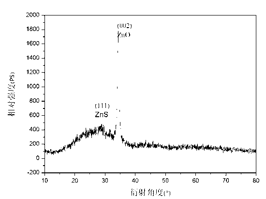
Figure 1 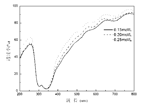
Figure 2 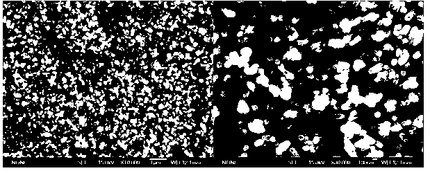
Figure 3
Abstract
Description
technical field
[0001] The invention relates to a method for preparing a window layer of a copper-zinc-tin-sulfur solar cell, belonging to the technical field of solar cell thin film device preparation technology. Background technique
[0002] Zinc oxide (ZnO) is a II-VI wide bandgap oxide semiconductor material with a bandwidth of about 3.37eV. It exhibits good n-type semiconductor performance and has good optoelectronic properties. ZnO has the characteristics of low preparation cost and low growth temperature, which is beneficial to reduce equipment cost, inhibit solid phase outdiffusion, improve film quality, and is easy to achieve doping. At the same time, the ZnO thin film is rich in raw materials, non-toxic, and has no pollution to the environment. It is an environmentally friendly material. Based on these excellent properties, ZnO can be used as a window material for solar cells.
[0003] Zinc sulfide (ZnS) is also a wide-bandgap semiconductor material with a bandgap...
Examples
Embodiment 1
[0022] A method for preparing a window layer of a copper-zinc-tin-sulfur solar cell, using a spin-coating method to prepare ZnO nano-array crystal seeds, using a hydrothermal method to grow a ZnO nano-array, and using a hydrothermal method to vulcanize and grow a ZnS shell structure, has the following process and step:
[0023] a) Cleaning of the glass substrate: Carry out surface cleaning treatment on the glass slide, put into triton aqueous solution, acetone solution, absolute alcohol solution and deionized water in order to sonicate for 15 minutes each, and then dry the glass slide.
[0024] b) Preparation of ZnO nanoarray seed crystals: ZnO seed crystals were prepared by spin coating method. Ethanolamine and zinc acetate are dissolved in ethanol at a concentration of 0.05mol / L, and are uniformly ultrasonicated. Put the glass slide substrate into the glue homogenizer, drop the seed crystal solution on the substrate with a dropper, the rotation speed is 1000 r / min, and the ...
Embodiment 2
[0028] The operation steps of this example are basically the same as those of Example 1, except that the concentration of TAA in the growth solution in step d) is 0.15 mol / L. Figure 4 is a scanning electron microscope image. The tip of the nanorod is in the shape of a hexagonal prism with a diameter of about 90nm.
Embodiment 3
[0030] The operation steps of this example are basically the same as those of Example 1, except that the concentration of TAA in the growth solution in step d) is 0.25 mol / L. Figure 5 is a scanning electron microscope image. The tip of the nanorod is in the shape of a hexagonal prism, and the diameter ranges from 120-140nm.