Chip and its manufacture method

A chip, preset direction technology, applied in electrical components, electrical solid devices, circuits, etc., can solve problems such as damage and chip yield impact

Inactive Publication Date: 2010-01-27
RAYDIUM SEMICON
View PDF3 Cites 0 Cited by
  • Summary
  • Abstract
  • Description
  • Claims
  • Application Information

AI Technical Summary

Problems solved by technology

[0004] On the other hand, the corner area of ​​the chip is often damaged by the stress generated by the packaging process, which affects the chip yield

Method used


Image

  • Chip and its manufacture method
  • Chip and its manufacture method
  • Chip and its manufacture method

Examples


Embodiment Construction

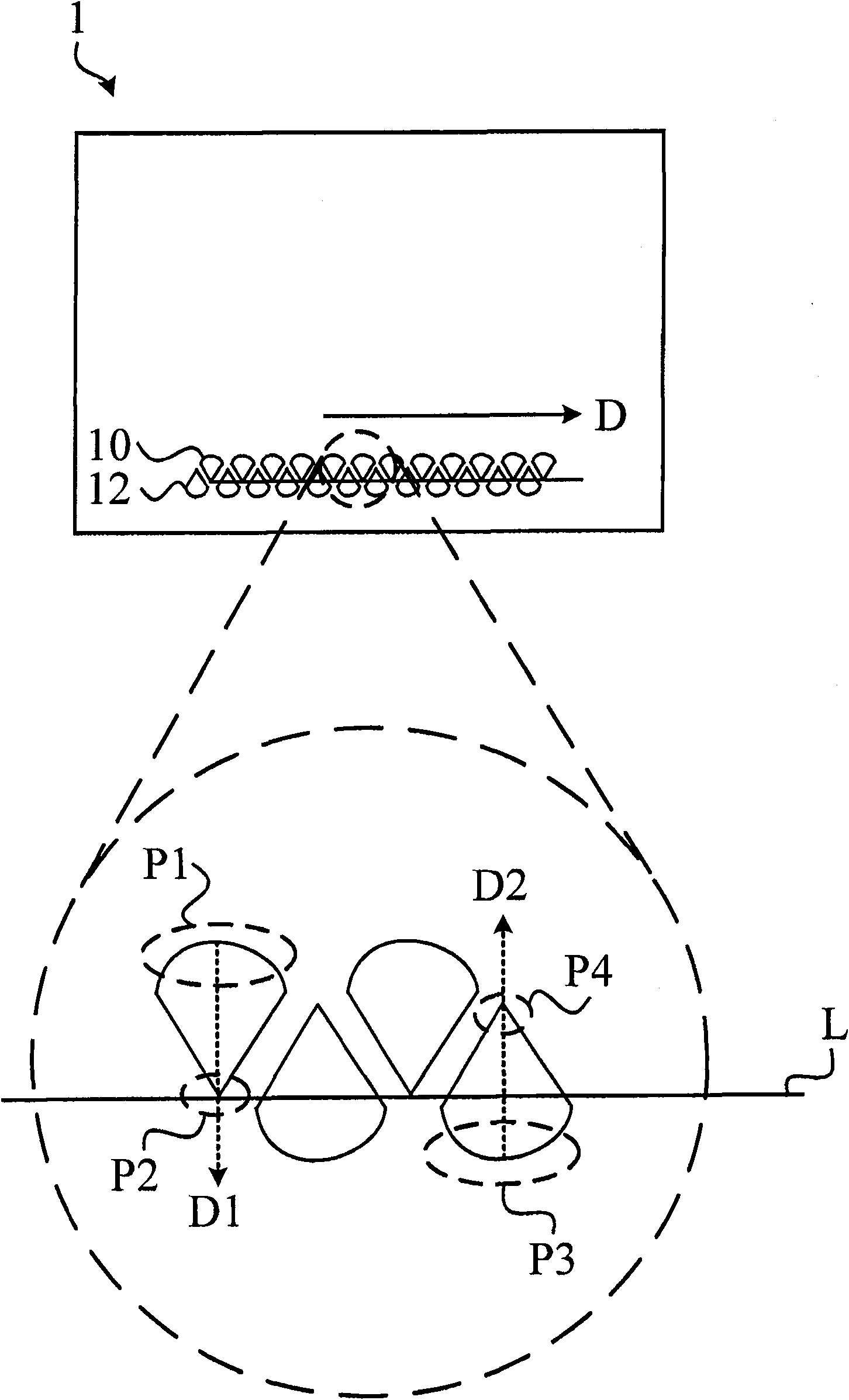
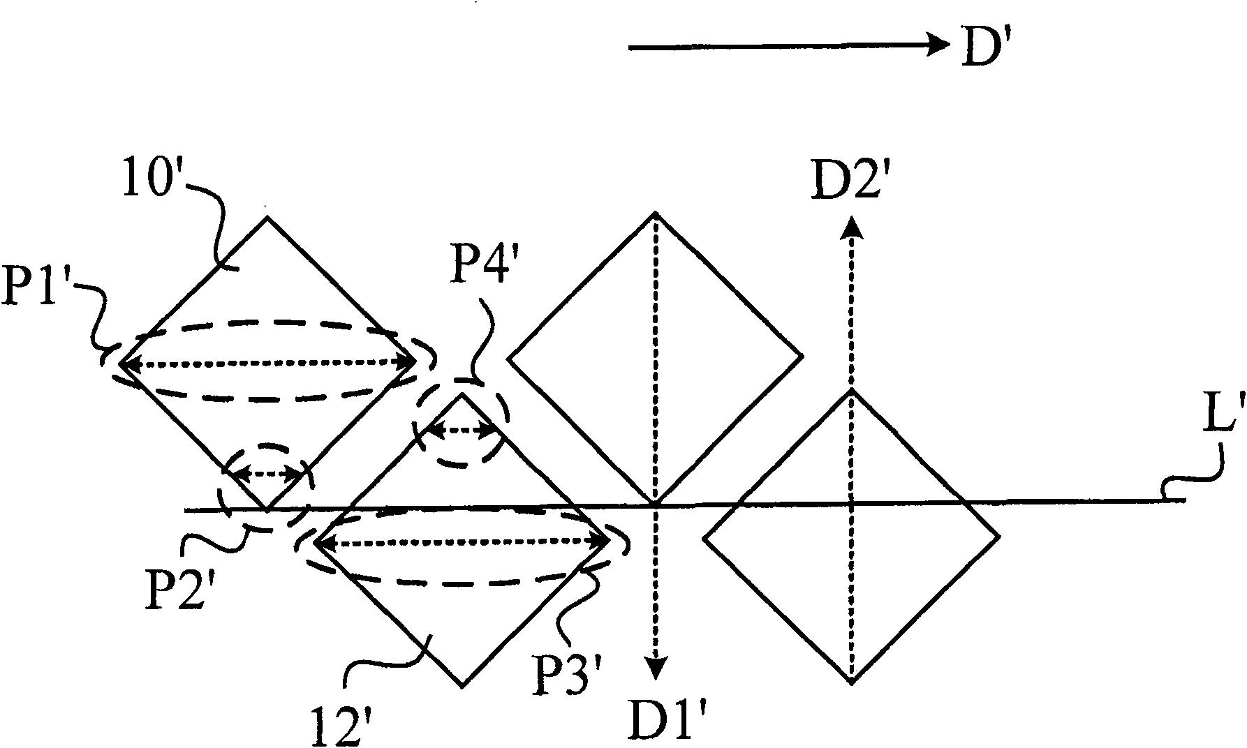
[0046] See Figure 2A , Figure 2A It is a schematic diagram of a chip 1 according to a specific embodiment of the present invention. Such as Figure 2A As shown, the chip 1 includes a plurality of first conductive pads 10 and a plurality of second conductive pads 12 having an approximately water drop shape. The first conductive pads 10 and the second conductive pads 12 are arranged alternately in the predetermined direction D, respectively. Each first conductive pad 10 includes a first portion P1 and a second portion P2 opposite to the first portion P1, and the length of the first portion P1 in the predetermined direction D is greater than the length of the second portion P2 in the predetermined direction D. Each second conductive pad 12 includes a third portion P3 and a fourth portion P4 opposite to the third portion P3, and the length of the third portion P3 in the predetermined direction D is greater than that of the fourth portion P4 in the predetermined direction D lengt...


PUM


Abstract

The invention discloses a chip and a manufacturing method thereof. The manufacturing method of the chip comprises the following steps: arranging a plurality of first conducting gaskets on the chip along one direction, wherein the first conducting gasket comprises a first part and a second part relative to the first part, and the length of the first part along the direction is larger than that of the second part along the direction; and arranging a plurality of second conducting gaskets arranged with the first conducting gaskets in a staggered manner on the chip, wherein each second conducting gasket comprises a third part and a fourth part relative to the third part, and the length of each third part along the direction is larger than that of the fourth part along the direction. The direction from the third part to the fourth part is opposite to the direction from the first part to the second part. The chip and the manufacturing method thereof can ensure that the conducting gaskets are densely arranged on the chip; and the design of the conducting gaskets at the corner can reduce the pressure damage of the chip generated during the encapsulation process.

Description

Technical field [0001] The present invention relates to a chip and a manufacturing method thereof, and in particular, the present invention relates to a chip and a manufacturing method thereof with a dense conductive gasket arrangement and a conductive gasket design that can reduce pressure damage at the corners of the chip. Background technique [0002] In recent years, due to the rapid development of semiconductor technology, the functions of chips have become more and more diversified. Correspondingly, the circuit design required for the function of the chip is becoming more and more complicated. Therefore, on a single chip, the number of conductive pads that act as contacts for providing electronic signals increases. When the number of conductive pads exceeds a certain level, it will inevitably directly affect the size of the chip, and reduce the number of chips that can be cut by a unit cell. In this way, the cost of chip production increases accordingly. Furthermore, over...

Claims


Application Information

Patent Timeline
Patent Type & Authority Patents(China)
IPC IPC(8): H01L23/485
CPCH01L24/05H01L24/06H01L2224/05552H01L2224/05554
Inventor 左克扬王威徐嘉宏周忠诚
Owner RAYDIUM SEMICON
Why Eureka
Try Eureka