Substrate and manufacturing method of package structure

a manufacturing method and packaging technology, applied in the direction of printed circuit manufacturing, printed circuit aspects, non-metallic protective coating applications, etc., can solve the problems of significant lowering of the yield rate of the package structure and increasing the manufacturing cost, so as to avoid oxidizing a first/second circuit structure, prevent the expansion of cracks, and reduce the damage of stress

Active Publication Date: 2011-11-01
ADVANCED SEMICON ENG INC
View PDF4 Cites 0 Cited by
  • Summary
  • Abstract
  • Description
  • Claims
  • Application Information

AI Technical Summary

Benefits of technology

[0013]The invention is directed to a substrate and a manufacturing method of a package structure using the same. A first / second solder mask exposes part of a cutting area, and part of a first / second solder mask is located on the cutting area for connecting the first / second inner area and the first / second outer area. As a result, the substrate and the manufacturing method of the package structure using the same at least includes advantages such as preventing the cracks from extending, reducing the damage of stress, avoiding oxidizing of a first / second circuit structure and preventing the first / second circuit structure from deforming or peeling off.

Problems solved by technology

The yield rate of the package structure is significantly lowered, and the manufacturing cost is increased.

Method used


Image

  • Substrate and manufacturing method of package structure
  • Substrate and manufacturing method of package structure
  • Substrate and manufacturing method of package structure

Examples


first embodiment

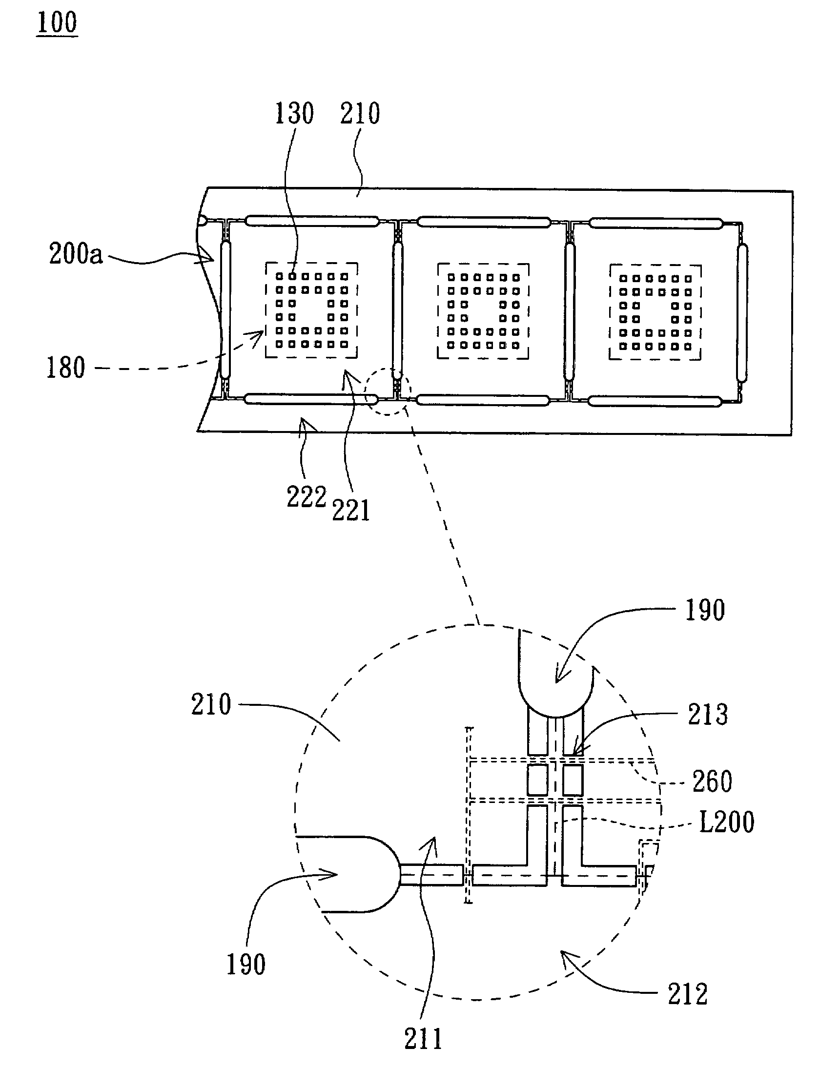
[0026]Please referring to FIG. 2A, a first surface 100a of a substrate 100 according to a first embodiment of the invention is illustrated in FIG. 2A. The substrate 100 includes the first surface 100a, a die-attaching area 180, a cutting area L100, several first pads 130 and a first solder mask 110. The die-attaching are 180 is for attaching a die (not shown in FIG. 2A). The first pads 130 are disposed on the first surface 100a. The first solder mask 110 is partially disposed on the first surface 100a and exposes part of the cutting area L100 and the first pads 130.

[0027]As shown in a dotted enlarge region in FIG. 2A, the first solder mask 110 is substantially divided into a first inner area 111 and a first outer area 112 via the cutting area L100. The die-attaching area 180 and the first pads 130 are located in the first inner area 111. Part of the first solder mask 110 is formed on the cutting area L100 for connecting the first inner area 111 and the first outer area 112.
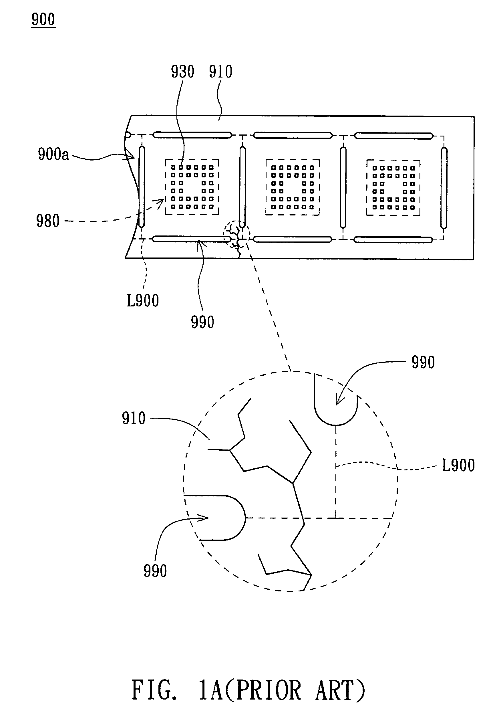
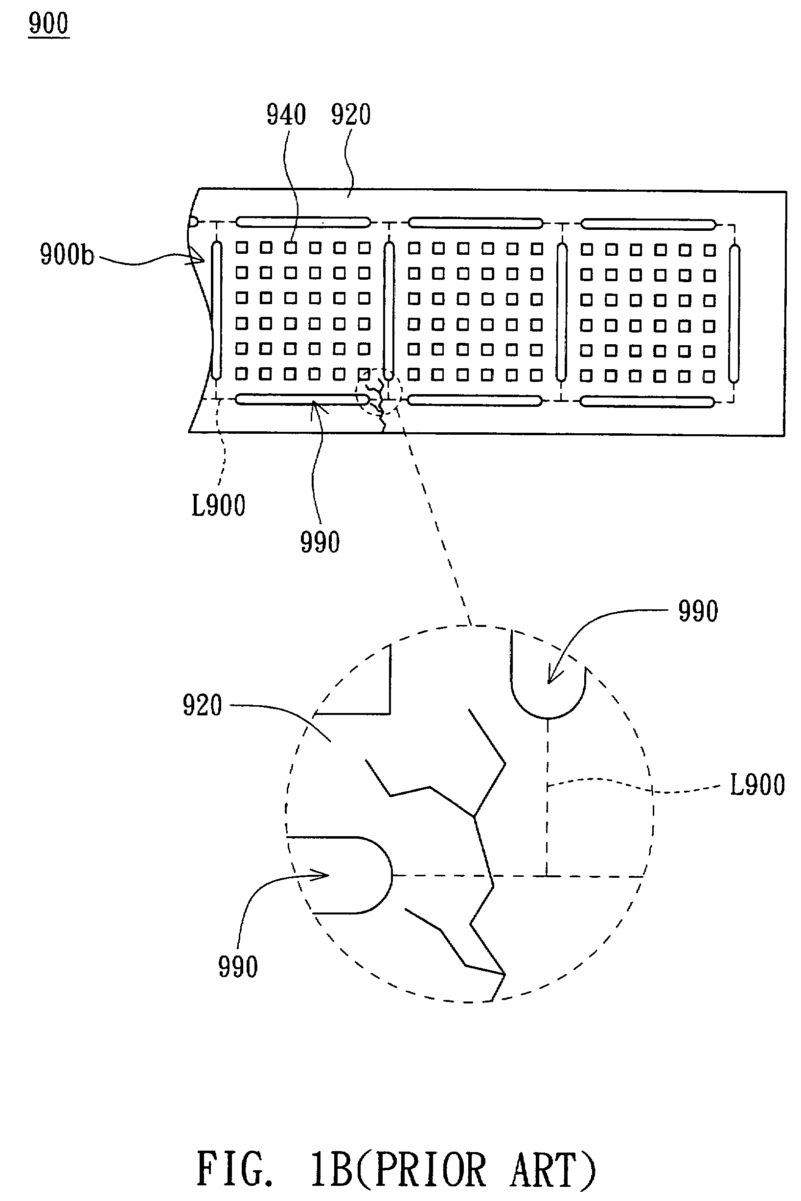
[0028]Whe...

second embodiment

[0047]A substrate 200 of the present embodiment and the substrate 100 of the first embodiment are different in the number of the first strip areas 213 and the second strip areas 223. The same parts are not illustrated repeatedly. Please refer to FIGS. 6A-6B. FIG. 6A illustrates a first surface 200a of a substrate 200 according to the second embodiment of the invention. FIG. 6B illustrates a second surface 200b of the substrate 200 according to the second embodiment of the invention.

[0048]As shown in FIG. 6A, the first solder mask 210 includes several first strip areas 213. The first strip areas 213 are substantially perpendicular to the cutting area L200 and connect the first inner area 211 and the first outer area 212. The first strip areas 213 cover the first circuit structure 260 in the substrate 200 for protecting the first circuit structure 260 from oxidization, deformation or peeling off.

[0049]As shown in FIG. 6B, the second solder mask 220 includes several second strip areas ...


PUM


Abstract

A substrate board and a manufacturing method of a package structure are provided. The substrate board includes a first surface, a die-attaching area, a cutting area, a plurality of first pads and a first solder mask. The die-attaching area for attaching a die is located on the first surface. The first pads are disposed on the first surface. The first solder mask is partially disposed on the first surface to expose part of the cutting area and the first pads. The first solder mask is divided into a first inner area and a first outer area via the cutting area. The die-attaching area and the first pads are located in the first inner area. Wherein, part of the first mask is located on the cutting area for connecting the first inner area and the first outer area.

Description

[0001]This application claims the benefit of Taiwan application Serial No. 095138268, filed Oct. 17, 2006, the subject matter of which is incorporated herein by reference.BACKGROUND OF THE INVENTION[0002]1. Field of the Invention[0003]The invention relates in general to a substrate and a manufacturing method of a package structure, and more particularly to a substrate with a solder mask exposing part of a cutting area and a manufacturing method of a package structure.[0004]2. Description of the Related Art[0005]As technology develops, all kinds of new electronic products enabling people to handle things more easy. The electronic products perform digital calculation through chips with micro-electric circuits, for providing all kinds of electric functions. The chip is disposed on a substrate and electrically connected to the substrate through wire-bonding or flip-chip bonding. Inner circuits of the chip are electrically connected to an outer circuit through the substrate. Furthermore,...

Claims


Application Information

Patent Timeline
Patent Type & Authority Patents(United States)
IPC IPC(8): H01L23/48
CPCH01L23/562H01L24/97H05K3/0052H01L23/3121H01L2924/00014H01L24/81H01L24/85H01L2224/16H01L2224/81801H05K3/242H05K3/28H05K2201/09036H05K2201/0909H05K2201/0989H05K2203/175H01L2924/01033H01L2224/85H01L2224/48H01L2224/45015H01L2924/207H01L2224/45099
Inventor CHANG, YUN-LUNGSUN, MING-WEI
Owner ADVANCED SEMICON ENG INC
Why Eureka
Try Eureka