
Implementing method and device of optical modulation

An implementation method and technology of optical modulation, applied in the field of optical modulation, can solve the problems of increased bit error rate due to bit errors, and achieve high reliability, cost saving, and easy-to-implement effects

Active Publication Date: 2010-05-12
HUAWEI TECH CO LTD
View PDF2 Cites 0 Cited by
  • Summary
  • Abstract
  • Description
  • Claims
  • Application Information

AI Technical Summary

Problems solved by technology

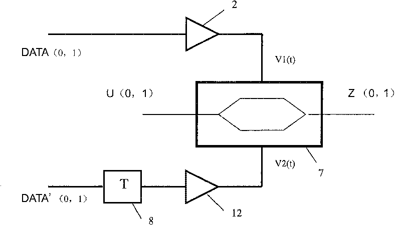
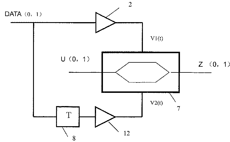
[0012] The present invention provides a method and device for realizing optical modulation, so as to solve the problems of bit errors and increased bit error rates that may be caused by the use of single-ended input and single-ended output delayers, and propose solutions to the problems Program

Method used


Image

  • Implementing method and device of optical modulation
  • Implementing method and device of optical modulation
  • Implementing method and device of optical modulation

Examples


Embodiment 1

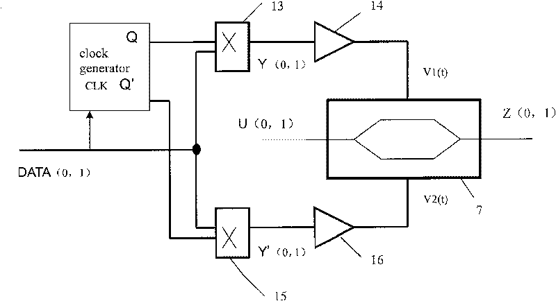
[0058] The clock generator in the second embodiment of the present invention uses the associated clock signal to generate the required clock sequence, so that when the input electrical signal data stream DATA(0, 1) passes through the clock generator, two complementary clock signals are generated. Compared with Embodiment 1 of the present invention, the advantage of this clock generator is that it can realize more clock sequences in various states as required.

[0059] Figure 5 The clock generator 2 in has two input ports: data signal input end I and clock signal input end CLK, and two output ports Q and Q', wherein two output ports Q and Q' output complementary, its working principle is based on T flip-flop as an example to illustrate, such as Figure 6 shown.

[0060] Figure 6 The clock signal 11 is input to the clock signal input terminal CLK of the T flip-flop, and the input electrical signal data stream 1 is input to the data signal input terminal I of the T flip-flop...


PUM


Abstract

A method for realizing optical modulation includes inputting two-path of complementary clock signals generated by passing input electric signal data through clock separately with input electric data stream together into the first and the second multiplication modules, inputting electric signal data streams outputted from the first and the second multiplication modules separately to high frequencyinput ends of modulator and carrying out modulation on optical signal by said modulator according to said electric signal data streams.

Description

technical field [0001] The invention relates to the field of communication transmission, in particular to an optical modulation implementation method and device suitable for an optical signal transmission system requiring high performance and long-term stability. Background technique [0002] In long-distance high-speed optical transmission systems, higher requirements are put forward for the spectrum utilization efficiency and dispersion tolerance of code patterns. The optical duo binary (ODB) modulation technology is a technology that converts a binary sequence into three special states according to certain rules in the optical domain to transmit optical signals. In the process of optical duobinary ODB modulation, three values ​​Z, A and B are used to represent the three logic states of duobinary: Z represents "0", A represents "1", and B represents "-1". These three values ​​can be three-level amplitude values ​​on the same phase, such as three-level amplitude modulation...

Claims


Application Information

Patent Timeline
Patent Type & Authority Patents(China)
IPC IPC(8): H04B10/18H04B10/155H04B10/516
Inventor 陶智慧
Owner HUAWEI TECH CO LTD
Learn More