Method for manufacturing semiconductor package structure having micro electro-mechanical system

A micro-electromechanical system and packaging structure technology, which is applied in semiconductor/solid-state device manufacturing, microstructure technology, semiconductor devices, etc., can solve problems such as increased production costs and high difficulty, and achieve increased production, reduced production costs, and application broad effect

CN101081692AActive Publication Date: 2007-12-05ADVANCED SEMICON ENG INC
0 Cites 6 Cited by

Patent Information

Authority / Receiving Office
CN · China
Patent Type
Applications(China)
Current Assignee / Owner
Publication Date
2007-12-05

Smart Images

  • Figure 1
    Figure 1
  • Figure 2
    Figure 2
  • Figure 3
    Figure 3
Patent Text Reader

Abstract

The process of manufacturing semiconductor package structure with micro electromechanical system includes the following steps: setting several micro electromechanical systems onto base plate units in one base plate, sealing these micro electromechanical systems with several covering bodies of one cover plate, eliminating the main body of the cover plate, and cutting the base plate to form several semiconductor package structures. The process has no need of forming locating markers and is simple. In addition, the cover plate has no need of being made of transparent material and the main body may be eliminated through a simple grinding step, so that the present invention has wide application and low production cost.
Need to check novelty before this filing date? Find Prior Art

Description

technical field

[0001] The present invention relates to a manufacturing method of a semiconductor packaging structure, and in particular to a manufacturing method of a semiconductor packaging structure with a micro-electromechanical system. Background technique

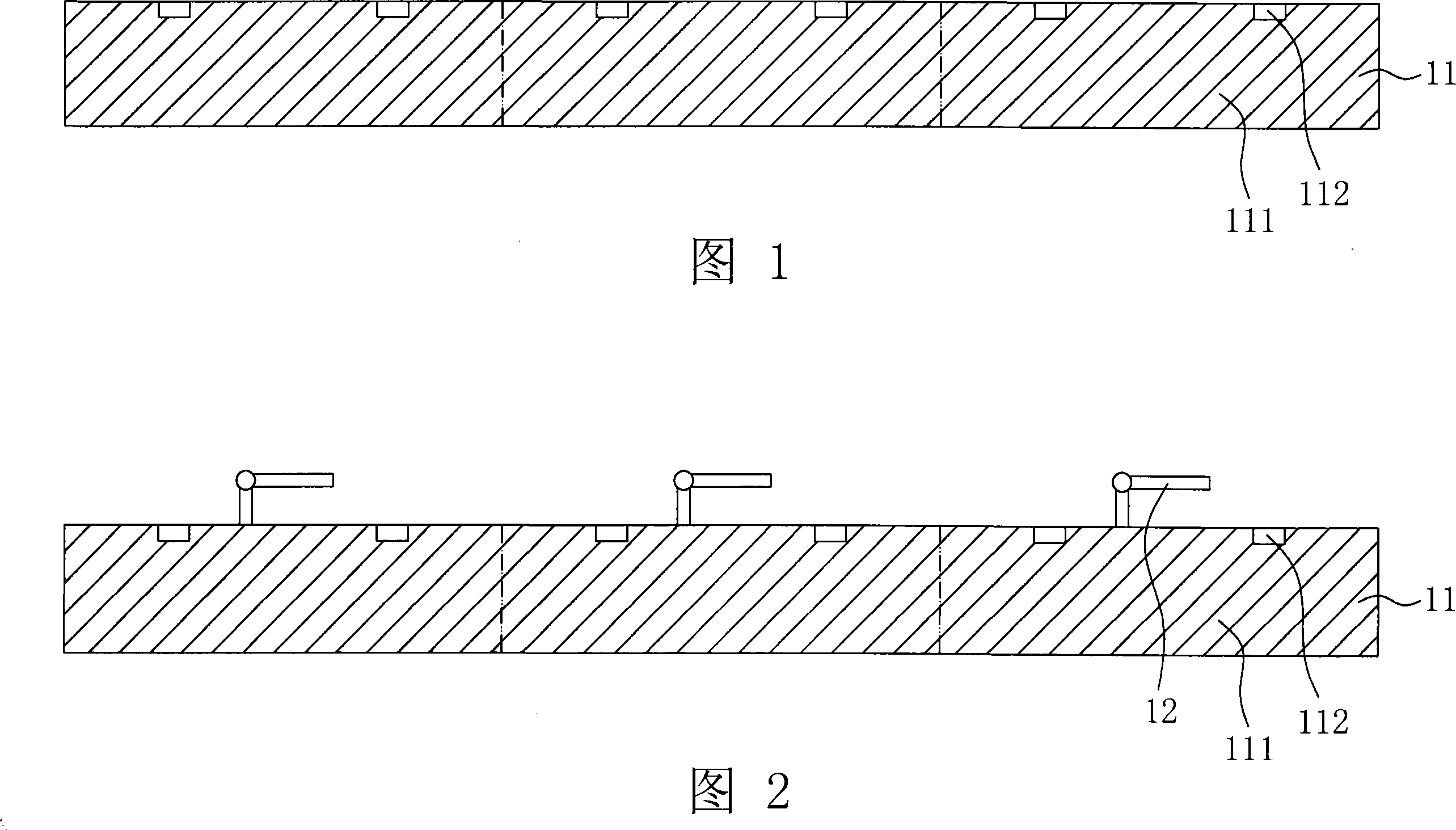
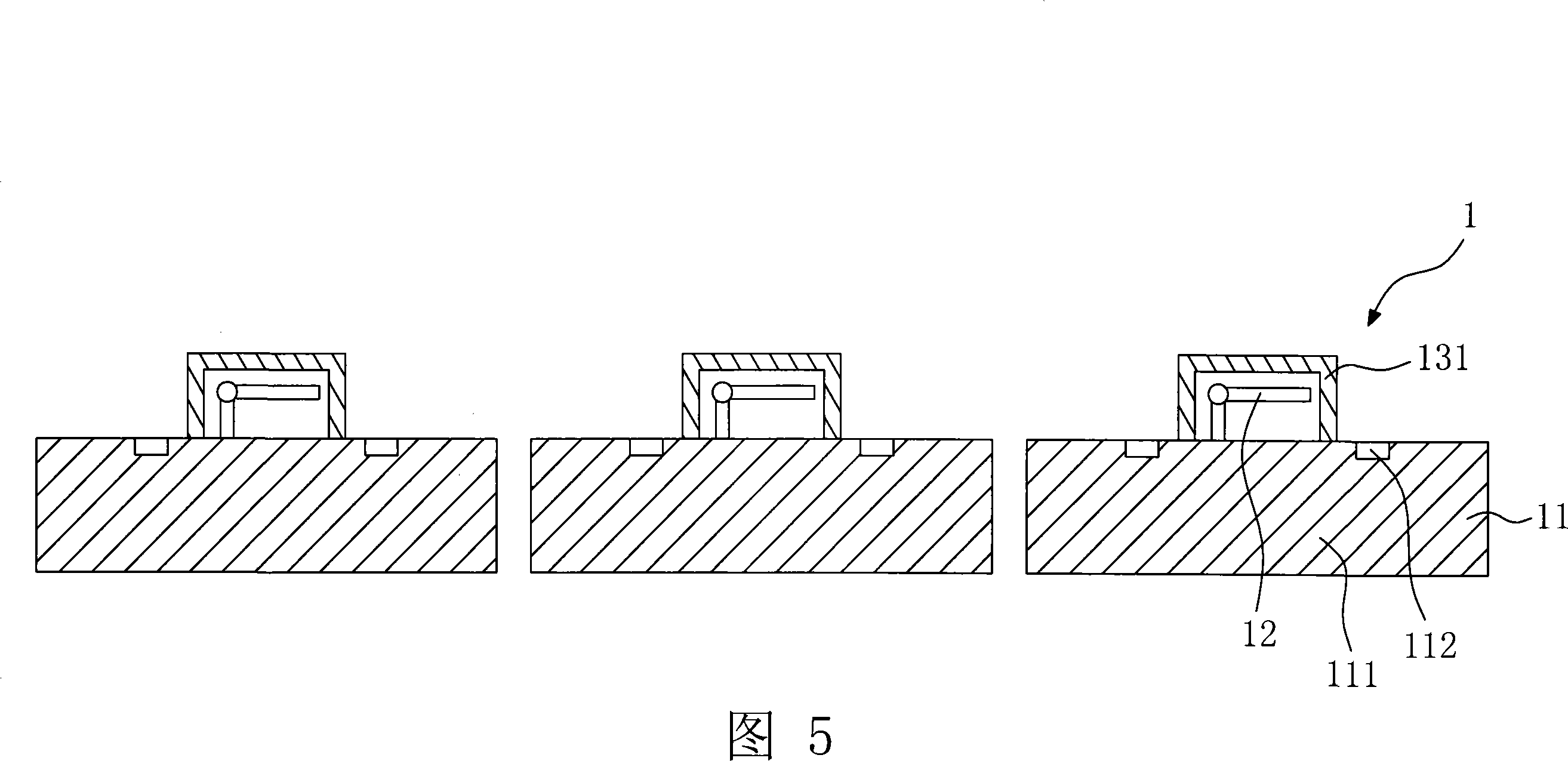
[0002] Please refer to FIG. 1 to FIG. 5 , which are schematic diagrams showing a conventional manufacturing method of a semiconductor package structure with micro-electro-mechanical systems (Micro-Electro-Mechanical Systems, MEMS). Please refer to FIG. 1 , firstly, a substrate 11 is provided, and the substrate 11 has a plurality of substrate units 111 (shown by dotted lines), and each substrate unit 111 has a plurality of pads 112 .

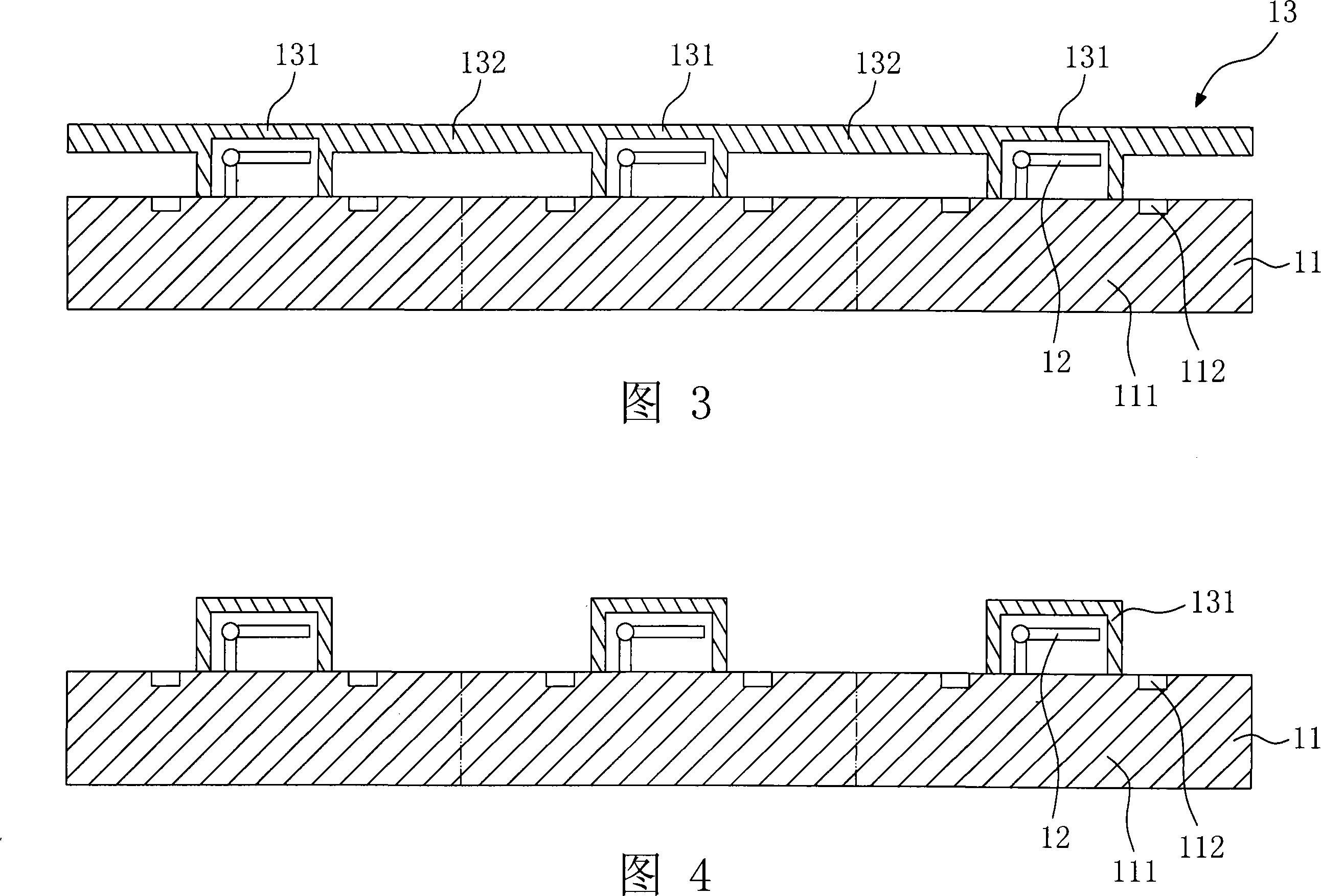
[0003] Referring to FIG. 2 , several MEMS 12 are disposed on each substrate unit 111 . Referring to FIG. 3 , a cover plate 13 is provided, and the cover plate 13 has a plurality of covers 131 and a plurality of connecting portions 132 , and the connecting portions 132 connect the cove...

Examples

Embodiment Construction

[0018] Referring to FIG. 6 to FIG. 10 , they are schematic diagrams of the manufacturing method of the semiconductor package structure with Micro-Electro-Mechanical Systems (MEMS) according to the present invention. Referring first to FIG. 6 , a substrate 21 is provided, and the substrate 21 has a plurality of substrate units 211 (shown by dotted lines), and each substrate unit 211 has a plurality of pads 212 . The substrate 21 can be a CMOS wafer.

[0019] Referring to FIG. 7 , a MEMS 22 is disposed on each substrate unit 211 . In this embodiment, the MEMS 22 is an optical element. The MEMS 22 includes at least one microlens set 221 , and each of the microlens sets 221 includes: a support member 222 , a hinge 223 and a microlens 224 . The support member 222 has a first end 225 and a second end 226 , wherein the second end 226 of the support member 222 is located on the substrate unit 211 . The hinge 223 is disposed on the first end 225 of the support member 222 . One end ...